
Lin Luo, Jun Liu, Guofang Wang, Yuxing Wu. Small-signal modeling and parameter extraction method for a multigate GaAs pHEMT switch[J]. Journal of Semiconductors, 2020, 41(3): 032102
- Journal of Semiconductors
- Vol. 41, Issue 3, 032102 (2020)
Abstract
1. Introduction
Currently, GaAs pHEMT switches play a more and more important role in RF switching and exhibit excellent performance in modern communication systems[
Accurate device modeling is a very important part of the semiconductor industry. For HEMT devices, the related research and literature have become popular, but generally only for common-source structures[
This paper presents a direct extraction method for GaAs pHEMT switches with a model that can be extended to multi-gate devices. In Section 2, the devices involved in this work and the related measurement instruments are introduced. The extraction process of the external parasitic parameters and intrinsic capacitor is described in detail in Section 3. Section 4 presents a verification of the model and a comparison of the simulated and measured data. Finally, the conclusions of this paper are presented.
2. Devices and instruments
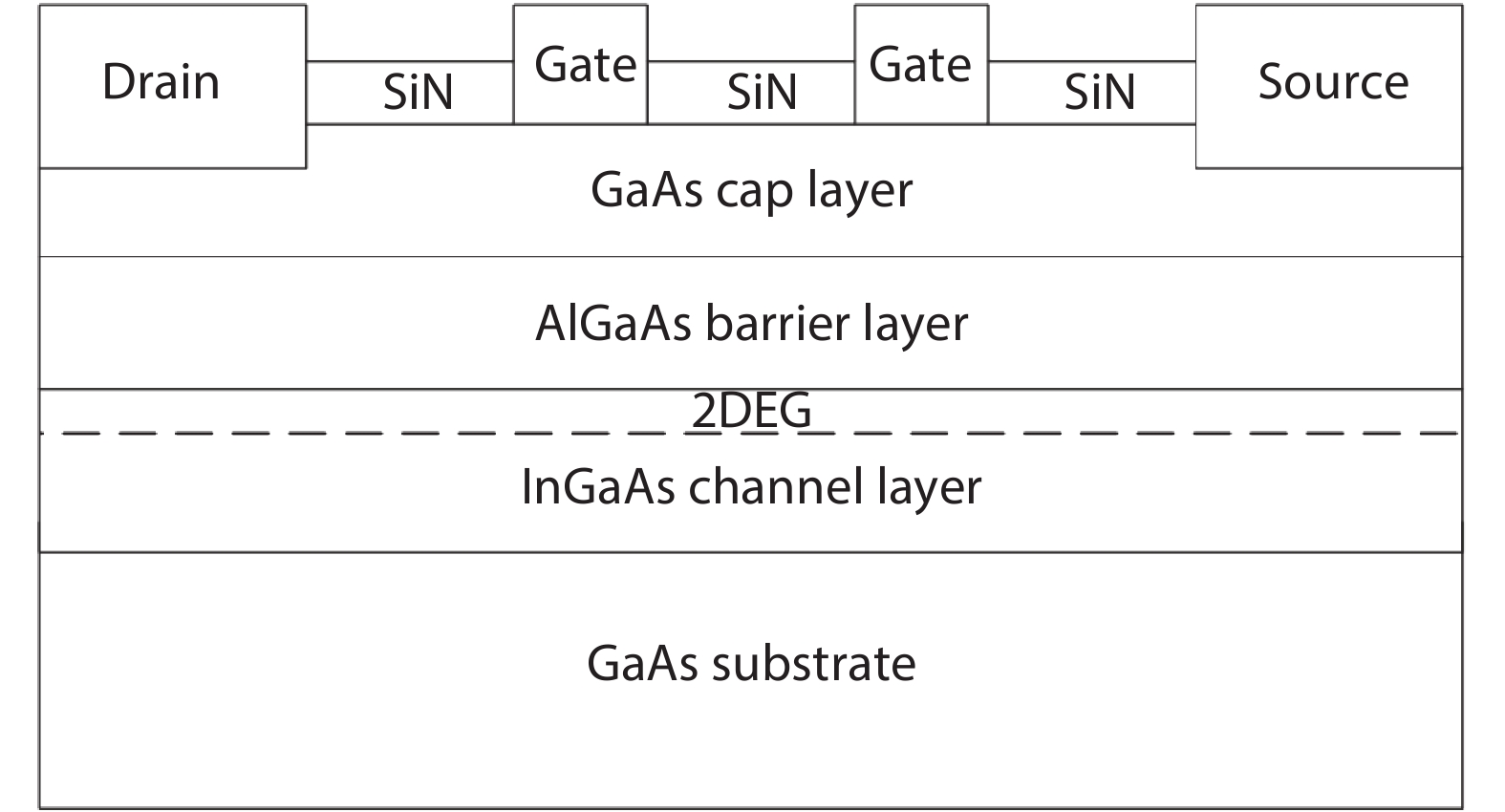
The GaAs pHEMT switches employed in this work include one switch with the normal common-gate GaAs pHEMT structure and a GaAs pHEMT switch whose gate is connected with a blocking resistor. In addition, the measured device includes a separate open structure for the extraction of the external parasitic capacitors. This device is grown on a 50 nm thick GaAs substrate as shown in Fig. 1, followed by a GaAs buffer layer to improve the effect of substrate defects of the channel. The channel is formed at the top of the InGaAs layer, and the electrons are provided by the upper AlGaAs layer. Ohmic contacts are created on the uppermost layer.
![]()
Figure 1.Cross-sectional structure of the dual-gate GaAs pHEMT switch.
Fig. 2 shows the layout of the dual-gate GaAs pHEMT switch. The gate length of the GaAs pHEMT switch is 0.5 µm, the total width is 625 μm (125 μm × 5), whose number of fingers is 5 with 125 μm finger width. and the value of the resistor switch connected to the gate is 20 kΩ. The multi-gate device is extended with dual, triple and quadruple gates. An advanced measurement system is used to characterize the considered GaAs pHEMT switches. The instruments in the measurement system include: a Cascade probe station, which can support on-chip testing; an Agilent 4156C DC power supply to provide a specific bias voltage to operate the switch at a specific voltage; and a Keysight vector network analyzer (VNA) for the two-part S parameter measurements for the model extraction and verification at 20 GHz.
![]()
Figure 2.(Color online) Layout of the dual-gate GaAs pHEMT switch(125
3. Extraction procedure
In this paper, the intrinsic structure of a multi-gate device can be represented by a series connection of the intrinsic structure of single-gate switches[
![]()
Figure 3.Small-signal equivalent circuit of the dual-gate GaAs pHEMT switch.
It is of great importance to accurately extract the external parasitic parameters in the modeling of small-signal models. An incomplete or exaggerated removal of the extrinsic capacitors influences the subsequently extracted elements and thus introduces errors. From the paper[
The imaginary part of the Y-parameters can be expressed with the following formula:
The extracted parameters via Eqs. (1)–(6) are shown in Fig. 4.
![]()
Figure 4.(Color online) Extracted parasitic capacitances versus frequency.
After de-embedding the effect of the pad parasitic capacitors, the other parasitic parameters can be extracted from the Z-parameters under the condition (Vds = 0 V, Vgs = 0 V). The equivalent topology is shown in Fig. 5. Rd, Rs and Rg are the parasitic resistors. Ld, Ls and Lg represent the parasitic inductors. Rds is the channel resistors, and Cb represents the effect of the gate capacitors, including Cgs, Cgd and Cgg*.
![]()
Figure 5.Equivalent circuit of the GaAs pHEMT switch under the condition (
The Z-parameters can be expressed as the following formula:
Since the blocking resistor RG = 20 kΩ prevents the leakage of RF signal, Lg and Rg can be ignored. The extracted parameters are shown in Fig. 6.
![]()
Figure 6.(Color online) Extracted parasitic inductors versus frequency.
After all of the external parasitic parameters have been removed, the intrinsic parameters can be accurately extracted. However, the gate is equivalent to an open circuit to the ground because the resistor RG prevents the leakage of RF signal. For this case, the equivalent circuit is shown in Fig. 7.
![]()
Figure 7.The intrinsic part with
Because the depletion layer under the gate is symmetric, it can be assumed that:
Rm is small enough to be ignored. At this time, the Y-parameters are expressed as follows:
Ytmp represents the intermediate variable of the admittance, and the specific form is as follows:
It can be obtained that:
Obviously, the intrinsic parameters cannot be extracted. Because the channel carrier under the gate is depleted in the deep-off-state, the intrinsic capacitors are mainly the fringe capacitance. The intrinsic capacitors (Cgs, Cgd and Cds) should be extracted from the GaAs pHEMT switch without the gate resistor RG. The device behaves as a common-gate structure of a pHEMT. With the effect of the inductor being ignored at low frequencies, considering only the imaginary part of the Y-parameter, the equivalent circuit is expressed as follows:
The extracted results via Eqs. (16)–(18) are shown in Fig. 8.
![]()
Figure 8.(Color online) Intrinsic capacitances versus frequency for the common-gate GaAs HEMT without
Under the same conditions, the channel resistors are extracted by the real part of the Y-parameter:
It is worth mentioning that the gate-to-gate capacitor Cgg* is adjusted to fit the off-state capacitor values. After all of the external parasitic parameters have been removed, considering only the imaginary part of the Y-parameter at low frequencies, the equivalent topology of the capacitors can be expressed as Fig. 9. The gate is equivalent to an open circuit to the ground. In the above extraction process, Cgs= Cgd= Cg is verified. Therefore, the imaginary part of Y11 can be derived as fellow:
![]()
Figure 9.Equivalent circuits of the dual-gate GaAs pHEMT switch.
Cgg* can be accurately extracted because Cg and Cds have been extracted from common-gate HEMTs.
Since all the extrinsic parasitic parameters are accurately extracted, the extracted intrinsic parameters hardly change with frequency. Table 1 summarizes the selection of the extracted values for the on and off states. So far, all the parameters of the dual-gate switch are extracted completely, and the verification of the model is discussed in the next section.
4. Model verification
The above extraction method is applied to extract the parameters of a GaAs HEMT switch with a measurement frequency range extending from 100 MHz to 20 GHz. Devices with dual, triple and quadruple gates are verified, considering a gate length of 0.5 µm and a gate total width of 625 µm (125 µm × 5). The fitting results of the GaAs HEMT switches are shown in Table 2.
Fig. 10 shows a comparison of the S-parameters between the simulation and the measurement of the on and off states in Smith charts. The agreements between the measured and simulated data are excellent over a wide frequency range.
![]()
Figure 10.(Color online) Comparison of the
The error formulations can be expressed using the following equations:
where Ssimuand Smeas represent the simulated and measured data sets, and n is the number of data points included in each data set. Table 3 shows the error percentage of different devices. The verification and accuracy are guaranteed. The percentage errors between the measured and simulated data are within 3%. Table 3 shows the different errors of each device.
The insertion loss and isolation results of the GaAs pHEMT multi-gate switch with a gate total width of 5 × 125 μm are shown in Fig. 11. The results of the modeling procedure fit the measurements well up to 20 GHz.
![]()
Figure 11.(Color online) Illustration of the simulated and measured insertion loss and isolation (0.1–20 GHz) for a device with a size of 5 × 125
5. Conclusion
A small-signal equivalent circuit for multi-gate GaAs pHEMTs in RF switching mode is proposed, and a direct extraction method is developed. By comparing the measured S-parameters with the model simulation results, it is found that the model provides high accuracy and strong reliability. Good fitting results for different gates also confirm the scalability of the extraction method. This extraction method can be applied to multi-gate GaAs pHEMT switch devices.
References
[1] H Tosaka, T Fujii, K Miyakoshi et al. An antenna switch MMIC using E/D mode p-HEMT for GSM/DCS/PCS/WCDMA bands application. IEEE MTT-S International Microwave Symposium Digest, 519(2003).
[2] H C Chiu, C S Cheng, C S Wu. Enhancement-and depletion-mode InGaP/InGaAs pHEMTs on 6-inch GaAs substrate. 2005 Asia-Pacific Microwave Conference Proceedings, 4(2005).
[3] A Khusro, M S Hashmi, A Q Ansari et al. An accurate and simplified small signal parameter extraction method for GaN HEMT. Int J Circuit Theory Appl, 47, 941(2019).
[4] Y Chen, Y Xu, Y Luo et al. A reliable and efficient small-signal parameter extraction method for GaN HEMTs. Int J Numer Model: Electron Networks, Devices Fields, e2540(2018).
[5] D V Bilevich, A A Popov, A S Salnikov et al. Automatic nonlinear modeling technique for GaAs HEMT. 2018 Dynamics of Systems, Mechanisms and Machines (Dynamics), 1(2018).
[6] L Yu, Y K Zheng, S Zhang et al. Small-signal model parameter extraction for AlGaN/GaN HEMT. J Semicond, 37, 034003(2016).
[7] G P Gibiino, A Santarelli, F Filicori. Charge-conservative GaN HEMT nonlinear modeling from non-isodynamic multi-bias
[8] W Changsi, X Yuehang, W Zhang et al. An improved temperature-dependent large signal model of microwave GaN HEMTs. J Semicond, 37, 074006(2016).
[9] W H Yu, S Y Yang, Y F Hou et al. Small signal model and low noise application of InAlAs/InGaAs/InP-based PHEMTS. J Infrared Millimeter Waves, 37, 683(2018).
[10] J Panda, K Jena, R Swain et al. Modeling on oxide dependent 2DEG sheet charge density and threshold voltage in AlGaN/GaN MOSHEMT. J Semicond, 37, 044003(2016).
[11] D K Panda, T R Lenka. Modeling and simulation of enhancement mode p-GaN Gate AlGaN/GaN HEMT for RF circuit switch applications. J Semicond, 38, 064002(2017).
[12] N Jain, R J Gutmann. Modeling and design of GaAs MESFET control devices for broad-band applications. IEEE Trans Microwave Theory Tech, 38, 109(1990).
[13] A Ehoud, L P Dunleavy, S C Lazar et al. Extraction techniques for FET switch modeling. IEEE Trans Microwave Theory Tech, 43, 1863(1995).
[14] S Takatani, C D Chen. Nonlinear steady-state III–V FET model for microwave antenna switch applications. IEEE Trans Electron Devices, 58, 4301(2011).
[15] Y Tao, Z F Hu, Y Fan et al. Direct extraction method of HEMT switch small-signal model with multiparasitic capacitive current path. Int J RF Microwave Comput-Aid Eng, 29, e21690(2019).
[16] M Geng, P X Li, W J Luo et al. Small-signal modeling of GaN HEMT switch with a new intrinsic elements extraction method. Chin Phys B, 25, 117301(2016).
[17] A R Alt, D Marti, C R Bolognesi. Transistor modeling: Robust small-signal equivalent circuit extraction in various HEMT technologies. IEEE Microwave Mag, 14, 83(2013).
[18] P M White, R M Healy. Improved equivalent circuit for determination of mesfet and hemt parasitic capacitors from "coldfet" measurements. IEEE Microwave Guided Wave Letts, 3, 453(1993).
[19] G Dambrine, A Cappy, F Heliodore et al. A new method for determining the FET small-signal equivalent circuit. IEEE Trans Microwave Theory Tech, 36, 1151(1988).

Set citation alerts for the article
Please enter your email address
© Copyright 2018-2021 | Chinese Laser Press. All Rights Reserved 沪ICP备15018463号-20