Contents


2024
Volume: 12 Issue 5
25 Article(s)
Export citation format
ADVANCING INTEGRATED PHOTONICS: FROM DEVICE INNOVATION TO SYSTEM INTEGRATION
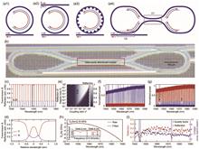
Reliable intracavity reflection for self-injection locking lasers and microcomb generation
Bitao Shen, Xuguang Zhang, Yimeng Wang, Zihan Tao, Haowen Shu, Huajin Chang, Wencan Li, Yan Zhou, Zhangfeng Ge, Ruixuan Chen, Bowen Bai, Lin Chang, and Xingjun Wang
Self-injection locking has emerged as a crucial technique for coherent optical sources, spanning from narrow linewidth lasers to the generation of localized microcombs. This technique involves key components, namely a laser diode and a high-quality cavity that induces narrow-band reflection back into the laser diode. However, in prior studies, the reflection mainly relied on the random intracavity Rayleigh backscattering, rendering it unpredictable and unsuitable for large-scale production and wide-band operation. In this work, we present a simple approach to achieve reliable intracavity reflection for self-injection locking to address this challenge by introducing a Sagnac loop into the cavity. This method guarantees robust reflection for every resonance within a wide operational band without compromising the quality factor or adding complexity to the fabrication process. As a proof of concept, we showcase the robust generation of narrow linewidth lasers and localized microcombs locked to different resonances within a normal-dispersion microcavity. Furthermore, the existence and generation of localized patterns in a normal-dispersion cavity with broadband forward–backward field coupling is first proved, as far as we know, both in simulation and in experiment. Our research offers a transformative approach to self-injection locking and holds great potential for large-scale production.Self-injection locking has emerged as a crucial technique for coherent optical sources, spanning from narrow linewidth lasers to the generation of localized microcombs. This technique involves key components, namely a laser diode and a high-quality cavity that induces narrow-band reflection back into the laser diode. However, in prior studies, the reflection mainly relied on the random intracavity Rayleigh backscattering, rendering it unpredictable and unsuitable for large-scale production and wide-band operation. In this work, we present a simple approach to achieve reliable intracavity reflection for self-injection locking to address this challenge by introducing a Sagnac loop into the cavity. This method guarantees robust reflection for every resonance within a wide operational band without compromising the quality factor or adding complexity to the fabrication process. As a proof of concept, we showcase the robust generation of narrow linewidth lasers and localized microcombs locked to different resonances within a normal-dispersion microcavity. Furthermore, the existence and generation of localized patterns in a normal-dispersion cavity with broadband forward–backward field coupling is first proved, as far as we know, both in simulation and in experiment. Our research offers a transformative approach to self-injection locking and holds great potential for large-scale production..
Photonics Research
- Publication Date: May. 01, 2024
- Vol. 12, Issue 5, A41 (2024)


Research Articles
Fiber Optics and Optical Communications

High power cladding-pumped low quantum defect Raman fiber amplifier
Yang Zhang, Jiangming Xu, Junrui Liang, Sicheng Li, Jun Ye, Xiaoya Ma, Tianfu Yao, Zhiyong Pan, Jinyong Leng, and Pu Zhou
Heat generated by the quantum defect (QD) in optically pumped lasers can result in detrimental effects such as mode instability, frequency noise, and even catastrophic damage. Previously, we demonstrated that boson-peak-based Raman fiber lasers have great potential in low QD laser generation. But their power scalability and heat load characteristics have yet to be investigated. Here, we demonstrate a boson-peak-based Raman fiber amplifier (RFA) with 815 W output power and a QD of 1.3%. The low heat generation characteristics of this low QD RFA are demonstrated. Both experimental and simulation results show that at this power level, the heat load of the low QD RFA is significantly lower than that of the conventional RFA with a QD of 4.8%. Thanks to its low heat generation characteristics, the proposed phosphosilicate-fiber-based low QD RFA provides an effective solution for the intractable thermal issue in optically pumped lasers, which is of significance in reducing the laser’s noise, improving the laser’s stability and safety, and solving the challenge of heat removing.Heat generated by the quantum defect (QD) in optically pumped lasers can result in detrimental effects such as mode instability, frequency noise, and even catastrophic damage. Previously, we demonstrated that boson-peak-based Raman fiber lasers have great potential in low QD laser generation. But their power scalability and heat load characteristics have yet to be investigated. Here, we demonstrate a boson-peak-based Raman fiber amplifier (RFA) with 815 W output power and a QD of 1.3%. The low heat generation characteristics of this low QD RFA are demonstrated. Both experimental and simulation results show that at this power level, the heat load of the low QD RFA is significantly lower than that of the conventional RFA with a QD of 4.8%. Thanks to its low heat generation characteristics, the proposed phosphosilicate-fiber-based low QD RFA provides an effective solution for the intractable thermal issue in optically pumped lasers, which is of significance in reducing the laser’s noise, improving the laser’s stability and safety, and solving the challenge of heat removing..
Photonics Research
- Publication Date: May. 01, 2024
- Vol. 12, Issue 5, 995 (2024)
Holography, Gratings, and Diffraction

Wide-angle digital holography with aliasing-free recording
Rafał Kukołowicz, Izabela Gerej, and Tomasz Kozacki
High-quality wide-angle holographic content is at the heart of the success of near-eye display technology. This work proposes the first digital holographic (DH) system enabling recording wide-angle scenes assembled from objects larger than the setup field of view (FOV), which can be directly replayed without 3D deformation in the near-eye display. The hologram formation in the DH system comprises free space propagation and Fourier transform (FT), which are connected by a rectangular aperture. First, the object wave propagates in free space to the rectangular aperture. Then, the band-limited wavefield is propagated through the single lens toward the camera plane. The rectangular aperture can take two sizes, depending on which DH operates in off-axis or phase-shifting recording mode. An integral part of the DH solution is a numerical reconstruction algorithm consisting of two elements: fringe processing for object wave recovery and wide-angle propagation to the object plane. The second element simulates propagation through both parts of the experimental system. The free space part is a space-limited angular spectrum compact space algorithm, while for propagation through the lens, the piecewise FT algorithm with Petzval curvature compensation is proposed. In the experimental part of the paper, we present the wide-angle DH system with FOV 25°×19°, which allows high-quality recording and reconstruction of large complex scenes.High-quality wide-angle holographic content is at the heart of the success of near-eye display technology. This work proposes the first digital holographic (DH) system enabling recording wide-angle scenes assembled from objects larger than the setup field of view (FOV), which can be directly replayed without 3D deformation in the near-eye display. The hologram formation in the DH system comprises free space propagation and Fourier transform (FT), which are connected by a rectangular aperture. First, the object wave propagates in free space to the rectangular aperture. Then, the band-limited wavefield is propagated through the single lens toward the camera plane. The rectangular aperture can take two sizes, depending on which DH operates in off-axis or phase-shifting recording mode. An integral part of the DH solution is a numerical reconstruction algorithm consisting of two elements: fringe processing for object wave recovery and wide-angle propagation to the object plane. The second element simulates propagation through both parts of the experimental system. The free space part is a space-limited angular spectrum compact space algorithm, while for propagation through the lens, the piecewise FT algorithm with Petzval curvature compensation is proposed. In the experimental part of the paper, we present the wide-angle DH system with FOV
Photonics Research
- Publication Date: May. 01, 2024
- Vol. 12, Issue 5, 1098 (2024)
Image Processing and Image Analysis

Complex transmission matrix retrieval for a highly scattering medium via regional phase differentiation
Qiaozhi He, Rongjun Shao, Yuan Qu, Linxian Liu, Chunxu Ding, and Jiamiao Yang
Accurately measuring the complex transmission matrix (CTM) of the scattering medium (SM) holds critical significance for applications in anti-scattering optical imaging, phototherapy, and optical neural networks. Non-interferometric approaches, utilizing phase retrieval algorithms, can robustly extract the CTM from the speckle patterns formed by multiple probing fields traversing the SM. However, in cases where an amplitude-type spatial light modulator is employed for probing field modulation, the absence of phase control frequently results in the convergence towards a local optimum, undermining the measurement accuracy. Here, we propose a high-accuracy CTM retrieval (CTMR) approach based on regional phase differentiation (RPD). It incorporates a sequence of additional phase masks into the probing fields, imposing a priori constraints on the phase retrieval algorithms. By distinguishing the variance of speckle patterns produced by different phase masks, the RPD-CTMR can effectively direct the algorithm towards a solution that closely approximates the CTM of the SM. We built a prototype of a digital micromirror device modulated RPD-CTMR. By accurately measuring the CTM of diffusers, we achieved an enhancement in the peak-to-background ratio of anti-scattering focusing by a factor of 3.6, alongside a reduction in the bit error rate of anti-scattering image transmission by a factor of 24. Our proposed approach aims to facilitate precise modulation of scattered optical fields, thereby fostering advancements in diverse fields including high-resolution microscopy, biomedical optical imaging, and optical communications.Accurately measuring the complex transmission matrix (CTM) of the scattering medium (SM) holds critical significance for applications in anti-scattering optical imaging, phototherapy, and optical neural networks. Non-interferometric approaches, utilizing phase retrieval algorithms, can robustly extract the CTM from the speckle patterns formed by multiple probing fields traversing the SM. However, in cases where an amplitude-type spatial light modulator is employed for probing field modulation, the absence of phase control frequently results in the convergence towards a local optimum, undermining the measurement accuracy. Here, we propose a high-accuracy CTM retrieval (CTMR) approach based on regional phase differentiation (RPD). It incorporates a sequence of additional phase masks into the probing fields, imposing a priori constraints on the phase retrieval algorithms. By distinguishing the variance of speckle patterns produced by different phase masks, the RPD-CTMR can effectively direct the algorithm towards a solution that closely approximates the CTM of the SM. We built a prototype of a digital micromirror device modulated RPD-CTMR. By accurately measuring the CTM of diffusers, we achieved an enhancement in the peak-to-background ratio of anti-scattering focusing by a factor of 3.6, alongside a reduction in the bit error rate of anti-scattering image transmission by a factor of 24. Our proposed approach aims to facilitate precise modulation of scattered optical fields, thereby fostering advancements in diverse fields including high-resolution microscopy, biomedical optical imaging, and optical communications..
Photonics Research
- Publication Date: Apr. 08, 2024
- Vol. 12, Issue 5, 876 (2024)
Instrumentation and Measurements

High-speed PGC demodulation model and method with subnanometer displacement resolution in a fiber-optic micro-probe laser interferometer
Yisi Dong, Wenwen Li, Jinran Zhang, Wenrui Luo, Haijin Fu, Xu Xing, Pengcheng Hu, Yongkang Dong, and Jiubin Tan
As the key of embedded displacement measurement, a fiber-optic micro-probe laser interferometer (FMI) is of great interest in developing high-end equipment as well as precision metrology. However, conventional phase-generated carrier (PGC) approaches are for low-speed scenes and local error analysis, usually neglecting the global precision analysis and dynamic effect of system parameters under high-speed measurement, thus hindering their broad applications. We present a high-speed PGC demodulation model and method to achieve subnanometer displacement measurement precision in FMI. This model includes a global equivalent resolution analysis and revelation of the demodulation error mechanism. Utilizing this model, the failure issues regarding the PGC demodulation method under high speed and large range are addressed. Furthermore, an ultra-precision PGC demodulation algorithm based on the combination of static and dynamic delay adaptive regulation is proposed to enable high-speed and large-range displacement measurement. In this paper, the proposed model and algorithm are validated through simulation and experimental tests. The results demonstrate a displacement resolution of 0.1 nm with a standard deviation of less than 0.5 nm when measuring at a high velocity of 1.5 m/s—nearly a tenfold increase of the latest study.As the key of embedded displacement measurement, a fiber-optic micro-probe laser interferometer (FMI) is of great interest in developing high-end equipment as well as precision metrology. However, conventional phase-generated carrier (PGC) approaches are for low-speed scenes and local error analysis, usually neglecting the global precision analysis and dynamic effect of system parameters under high-speed measurement, thus hindering their broad applications. We present a high-speed PGC demodulation model and method to achieve subnanometer displacement measurement precision in FMI. This model includes a global equivalent resolution analysis and revelation of the demodulation error mechanism. Utilizing this model, the failure issues regarding the PGC demodulation method under high speed and large range are addressed. Furthermore, an ultra-precision PGC demodulation algorithm based on the combination of static and dynamic delay adaptive regulation is proposed to enable high-speed and large-range displacement measurement. In this paper, the proposed model and algorithm are validated through simulation and experimental tests. The results demonstrate a displacement resolution of 0.1 nm with a standard deviation of less than 0.5 nm when measuring at a high velocity of 1.5 m/s—nearly a tenfold increase of the latest study..
Photonics Research
- Publication Date: May. 01, 2024
- Vol. 12, Issue 5, 921 (2024)

Dead-zone-free atomic magnetometer based on hybrid Poincaré beams
Ke Tian, Weifeng Ding, and Zhaoying Wang
In this paper, we present the experiment and the theory scheme of light-atom interaction in atomic magnetometers by using a hybrid Poincaré beam (HPB) to solve an annoying problem, named “dead zone.” This kind of magnetometer can be sensitive to arbitrary directions of external magnetic fields. The HPB has a complex polarization distribution, consisting of a vector radially polarized beam and a scalar circularly polarized beam in our experiment. These two kinds of beams have different directions of dead zones of external magnetic fields; thereby, the atomic magnetometer with an HPB can avoid the non-signal area when the direction of the external magnetic field is in the plane perpendicular to the light polarization plane. Furthermore, the optical magnetic resonance (OMR) signal using an HPB still has no dead zones even when the direction of the external magnetic field is in the plane parallel to the polarization plane in our scheme. Our work has the potential to simplify and optimize dead-zone-free atomic magnetometers.In this paper, we present the experiment and the theory scheme of light-atom interaction in atomic magnetometers by using a hybrid Poincaré beam (HPB) to solve an annoying problem, named “dead zone.” This kind of magnetometer can be sensitive to arbitrary directions of external magnetic fields. The HPB has a complex polarization distribution, consisting of a vector radially polarized beam and a scalar circularly polarized beam in our experiment. These two kinds of beams have different directions of dead zones of external magnetic fields; thereby, the atomic magnetometer with an HPB can avoid the non-signal area when the direction of the external magnetic field is in the plane perpendicular to the light polarization plane. Furthermore, the optical magnetic resonance (OMR) signal using an HPB still has no dead zones even when the direction of the external magnetic field is in the plane parallel to the polarization plane in our scheme. Our work has the potential to simplify and optimize dead-zone-free atomic magnetometers..
Photonics Research
- Publication Date: May. 01, 2024
- Vol. 12, Issue 5, 1093 (2024)
Integrated Optics

Highly efficient fiber to Si waveguide free-form coupler for foundry-scale silicon photonics | Editors' Pick
Luigi Ranno, Jia Xu Brian Sia, Cosmin Popescu, Drew Weninger, Samuel Serna, Shaoliang Yu, Lionel C. Kimerling, Anuradha Agarwal, Tian Gu, and Juejun Hu
As silicon photonics transitions from research to commercial deployment, packaging solutions that efficiently couple light into highly compact and functional sub-micrometer silicon waveguides are imperative but remain challenging. The 220 nm silicon-on-insulator (SOI) platform, poised to enable large-scale integration, is the most widely adopted by foundries, resulting in established fabrication processes and extensive photonic component libraries. The development of a highly efficient, scalable, and broadband coupling scheme for this platform is therefore of paramount importance. Leveraging two-photon polymerization (TPP) and a deterministic free-form micro-optics design methodology based on the Fermat’s principle, this work demonstrates an ultra-efficient and broadband 3-D coupler interface between standard SMF-28 single-mode fibers and silicon waveguides on the 220 nm SOI platform. The coupler achieves a low coupling loss of 0.8 dB for the fundamental TE mode, along with 1 dB bandwidth exceeding 180 nm. The broadband operation enables diverse bandwidth-driven applications ranging from communications to spectroscopy. Furthermore, the 3-D free-form coupler also enables large tolerance to fiber misalignments and manufacturing variability, thereby relaxing packaging requirements toward cost reduction capitalizing on standard electronic packaging process flows.As silicon photonics transitions from research to commercial deployment, packaging solutions that efficiently couple light into highly compact and functional sub-micrometer silicon waveguides are imperative but remain challenging. The 220 nm silicon-on-insulator (SOI) platform, poised to enable large-scale integration, is the most widely adopted by foundries, resulting in established fabrication processes and extensive photonic component libraries. The development of a highly efficient, scalable, and broadband coupling scheme for this platform is therefore of paramount importance. Leveraging two-photon polymerization (TPP) and a deterministic free-form micro-optics design methodology based on the Fermat’s principle, this work demonstrates an ultra-efficient and broadband 3-D coupler interface between standard SMF-28 single-mode fibers and silicon waveguides on the 220 nm SOI platform. The coupler achieves a low coupling loss of 0.8 dB for the fundamental TE mode, along with 1 dB bandwidth exceeding 180 nm. The broadband operation enables diverse bandwidth-driven applications ranging from communications to spectroscopy. Furthermore, the 3-D free-form coupler also enables large tolerance to fiber misalignments and manufacturing variability, thereby relaxing packaging requirements toward cost reduction capitalizing on standard electronic packaging process flows..
Photonics Research
- Publication Date: May. 01, 2024
- Vol. 12, Issue 5, 1055 (2024)
Lasers and Laser Optics
Perovskite quantum laser with enhanced population inversion driven by plasmon-induced hot electron transfer under potential shift polarization conditions
Yong Pan, Lijie Wu, Yuan Zhang, Yihao Zhang, Jie Xu, Haixia Xie, and Jianguo Cao
The hot electron transfer resulting in fluorescence enhancement is significantly meaningful for theory and experiment of the study on photoelectric devices. However, the laser emission based on direct hot electron transfer is difficult to realize because of the low transfer efficiency. To achieve a laser with a new-generation mechanism based on hot electron transfer, the photoelectric co-excitation is proposed for improving the efficiency of hot electron transfer. The lasing behavior at 532 nm is realized with a threshold of 5 kw cm-2 and 1 μA, which can be considered as the hot electron transfer resulting in population inversion enhancement. Meanwhile, the lasing output power is 0.3 mW. The hot electrons transfer process was described via the transient absorption spectrum according to the improved ground-state bleaching and excited-state absorption signal in device ON. Through comparison with the optical pump only, the quantum efficiencies of hot electron generation (HEG) and hot electron transfer (HET) were increased ∼31% and 31%, respectively. Most importantly, a triple gain mode coupling device including local surface plasmon, hot electron transfer, and array oscillation was presented. Two modes of population inversion enhancement are proposed. This study can provide theoretical and experimental reference for the research of hot electron lasers and devices.The hot electron transfer resulting in fluorescence enhancement is significantly meaningful for theory and experiment of the study on photoelectric devices. However, the laser emission based on direct hot electron transfer is difficult to realize because of the low transfer efficiency. To achieve a laser with a new-generation mechanism based on hot electron transfer, the photoelectric co-excitation is proposed for improving the efficiency of hot electron transfer. The lasing behavior at 532 nm is realized with a threshold of
Photonics Research
- Publication Date: May. 01, 2024
- Vol. 12, Issue 5, 986 (2024)
Medical Optics and Biotechnology
Enriched photosensitizer for deep-seated-tumor photodynamic therapy
Hongrui Shan, Xueqian Wang, Qiheng Wei, Hailang Dai, and Xianfeng Chen
Photodynamic therapy (PDT) is an innovative approach that utilizes photochemical reactions for non-invasive disease treatment. Conventional PDT is limited by the low penetration depth of visible light required for activation. Herein, we employed upconversion nanoparticles (UCNPs) to extend the activation wavelength of photosensitizers into the infrared range, enabling a treatment depth of over 10 mm. Furthermore, we also used the abundant amino groups of branched polyethyleneimine (PEI) with spatial structure to enhance the loading capacity of protoporphyrin (PPIX), and we ultimately improved skin tumor clearance rates. Moreover, we achieved tumor-specific treatment by utilizing folic acid (FA) targeting and active enrichment of PPIX. According to cellular experimental results, we demonstrated the remarkable reactive oxygen species generation capability of the material and ultra-low dark toxicity. Additionally, we investigated the apoptosis mechanism and demonstrated that the synthesized nanoparticle stimulates the up-regulation of apoptosis-associated proteins Bax/Bcl-2 and Cyto c. During in vivo experiments involving intravenous injection in mouse tails, we investigated the anticancer efficacy of the nanoparticle, confirming its excellent PDT effects. This research provides a promising avenue for future non-invasive treatment of deep-seated tumors, offering a method for the treatment and management of specific cancers.Photodynamic therapy (PDT) is an innovative approach that utilizes photochemical reactions for non-invasive disease treatment. Conventional PDT is limited by the low penetration depth of visible light required for activation. Herein, we employed upconversion nanoparticles (UCNPs) to extend the activation wavelength of photosensitizers into the infrared range, enabling a treatment depth of over 10 mm. Furthermore, we also used the abundant amino groups of branched polyethyleneimine (PEI) with spatial structure to enhance the loading capacity of protoporphyrin (PPIX), and we ultimately improved skin tumor clearance rates. Moreover, we achieved tumor-specific treatment by utilizing folic acid (FA) targeting and active enrichment of PPIX. According to cellular experimental results, we demonstrated the remarkable reactive oxygen species generation capability of the material and ultra-low dark toxicity. Additionally, we investigated the apoptosis mechanism and demonstrated that the synthesized nanoparticle stimulates the up-regulation of apoptosis-associated proteins Bax/Bcl-2 and Cyto c. During in vivo experiments involving intravenous injection in mouse tails, we investigated the anticancer efficacy of the nanoparticle, confirming its excellent PDT effects. This research provides a promising avenue for future non-invasive treatment of deep-seated tumors, offering a method for the treatment and management of specific cancers..
Photonics Research
- Publication Date: May. 01, 2024
- Vol. 12, Issue 5, 1024 (2024)
Nanophotonics and Photonic Crystals
Optical trapping-enhanced probes designed by a deep learning approach
Miao Peng, Guangzong Xiao, Xinlin Chen, Te Du, Tengfang Kuang, Xiang Han, Wei Xiong, Gangyi Zhu, Junbo Yang, Zhongqi Tan, Kaiyong Yang, and Hui Luo
Realizing optical trapping enhancement is crucial in biomedicine, fundamental physics, and precision measurement. Taking the metamaterials with artificially engineered permittivity as photonic force probes in optical tweezers will offer unprecedented opportunities for optical trap enhancement. However, it usually involves multi-parameter optimization and requires lengthy calculations; thereby few studies remain despite decades of research on optical tweezers. Here, we introduce a deep learning (DL) model to attack this problem. The DL model can efficiently predict the maximum axial optical stiffness of Si/Si3N4 (SSN) multilayer metamaterial nanoparticles and reduce the design duration by about one order of magnitude. We experimentally demonstrate that the designed SSN nanoparticles show more than twofold and fivefold improvement in the lateral (kx and ky) and the axial (kz) optical trap stiffness on the high refractive index amorphous TiO2 microsphere. Incorporating the DL model in optical manipulation systems will expedite the design and optimization processes, providing a means for developing various photonic force probes with specialized functional behaviors.Realizing optical trapping enhancement is crucial in biomedicine, fundamental physics, and precision measurement. Taking the metamaterials with artificially engineered permittivity as photonic force probes in optical tweezers will offer unprecedented opportunities for optical trap enhancement. However, it usually involves multi-parameter optimization and requires lengthy calculations; thereby few studies remain despite decades of research on optical tweezers. Here, we introduce a deep learning (DL) model to attack this problem. The DL model can efficiently predict the maximum axial optical stiffness of
Photonics Research
- Publication Date: May. 01, 2024
- Vol. 12, Issue 5, 959 (2024)
Optical magnetic field enhancement using ultrafast azimuthally polarized laser beams and tailored metallic nanoantennas
Rodrigo Martín-Hernández, Lorenz Grünewald, Luis Sánchez-Tejerina, Luis Plaja, Enrique Conejero Jarque, Carlos Hernández-García, and Sebastian Mai
Structured light provides unique opportunities to spatially tailor the electromagnetic field of laser beams. These include the possibility of a sub-wavelength spatial separation of their electric and magnetic fields, which would allow isolating interactions of matter with pure magnetic (or electric) fields. This could be particularly interesting in molecular spectroscopy, as excitations due to electric and—usually very weak—magnetic transition dipole moments can be disentangled. In this work, we show that the use of tailored metallic nanoantennas drastically enhances the strength of the longitudinal magnetic field carried by an ultrafast azimuthally polarized beam (by a factor of ∼65), which is spatially separated from the electric field by the beam’s symmetry. Such enhancement is due to favorable phase-matching of the magnetic field induced by the electric current loops created in the antennas. Our particle-in-cell simulation results demonstrate that the interactions of moderately intense (∼1011 W/cm2) and ultrafast azimuthally polarized laser beams with conical, parabolic, Gaussian, or logarithmic metallic nanoantennas provide spatially isolated magnetic field pulses of several tens of Tesla.Structured light provides unique opportunities to spatially tailor the electromagnetic field of laser beams. These include the possibility of a sub-wavelength spatial separation of their electric and magnetic fields, which would allow isolating interactions of matter with pure magnetic (or electric) fields. This could be particularly interesting in molecular spectroscopy, as excitations due to electric and—usually very weak—magnetic transition dipole moments can be disentangled. In this work, we show that the use of tailored metallic nanoantennas drastically enhances the strength of the longitudinal magnetic field carried by an ultrafast azimuthally polarized beam (by a factor of
Photonics Research
- Publication Date: May. 01, 2024
- Vol. 12, Issue 5, 1078 (2024)
Nonlinear Optics
Nonlinear generation of vector beams by using a compact nonlinear fork grating
Qian Yang, Yangfeifei Yang, Hao Li, Haigang Liu, and Xianfeng Chen
Vectorial beams have attracted great interest due to their broad applications in optical micromanipulation, optical imaging, optical micromachining, and optical communication. Nonlinear frequency conversion is an effective technique to expand the frequency range of the vectorial beams. However, the scheme of existing methods to generate vector beams of the second harmonic (SH) lacks compactness in the experiment. Here, we introduce a new way to realize the generation of vector beams of SH by using a nonlinear fork grating to solve such a problem. We examine the properties of generated SH vector beams by using Stokes parameters, which agree well with theoretical predictions. Then we demonstrate that linearly polarized vector beams with arbitrary topological charge can be achieved by adjusting the optical axis direction of the half-wave plate (HWP). Finally, we measure the nonlinear conversion efficiency of such a method. The proposed method provides a new way to generate vector beams of SH by using a microstructure of nonlinear crystal, which may also be applied in other nonlinear processes and promote all-optical waveband applications of such vector beams.Vectorial beams have attracted great interest due to their broad applications in optical micromanipulation, optical imaging, optical micromachining, and optical communication. Nonlinear frequency conversion is an effective technique to expand the frequency range of the vectorial beams. However, the scheme of existing methods to generate vector beams of the second harmonic (SH) lacks compactness in the experiment. Here, we introduce a new way to realize the generation of vector beams of SH by using a nonlinear fork grating to solve such a problem. We examine the properties of generated SH vector beams by using Stokes parameters, which agree well with theoretical predictions. Then we demonstrate that linearly polarized vector beams with arbitrary topological charge can be achieved by adjusting the optical axis direction of the half-wave plate (HWP). Finally, we measure the nonlinear conversion efficiency of such a method. The proposed method provides a new way to generate vector beams of SH by using a microstructure of nonlinear crystal, which may also be applied in other nonlinear processes and promote all-optical waveband applications of such vector beams..
Photonics Research
- Publication Date: May. 01, 2024
- Vol. 12, Issue 5, 1036 (2024)
Optical and Photonic Materials
Ultrafast modulable 2DEG Huygens metasurface | Spotlight on Optics
Hongxin Zeng, Xuan Cong, Shiqi Wang, Sen Gong, Lin Huang, Lan Wang, Huajie Liang, Feng Lan, Haoyi Cao, Zheng Wang, Weipeng Wang, Shixiong Liang, Zhihong Feng, Ziqiang Yang, Yaxin Zhang, and Tie Jun Cui
Huygens metasurfaces have demonstrated remarkable potential in perfect transmission and precise wavefront modulation through the synergistic integration of electric resonance and magnetic resonance. However, prevailing active or reconfigurable Huygens metasurfaces, based on all-optical systems, encounter formidable challenges associated with the intricate control of bulk dielectric using laser equipment and the presence of residual thermal effects, leading to limitations in continuous modulation speeds. Here, we present an ultrafast electrically driven terahertz Huygens metasurface that comprises an artificial microstructure layer featuring a two-dimensional electron gas (2DEG) provided by an AlGaN/GaN heterojunction, as well as a passive microstructure layer. Through precise manipulation of the carrier concentration within the 2DEG layer, we effectively govern the current distribution on the metasurfaces, inducing variations in electromagnetic resonance modes to modulate terahertz waves. This modulation mechanism achieves high efficiency and contrast for terahertz wave manipulation. Experimental investigations demonstrate continuous modulation capabilities of up to 6 GHz, a modulation efficiency of 90%, a transmission of 91%, and a remarkable relative operating bandwidth of 55.5%. These significant advancements substantially enhance the performance of terahertz metasurface modulators. Importantly, our work not only enables efficient amplitude modulation but also introduces an approach for the development of high-speed and efficient intelligent transmissive metasurfaces.Huygens metasurfaces have demonstrated remarkable potential in perfect transmission and precise wavefront modulation through the synergistic integration of electric resonance and magnetic resonance. However, prevailing active or reconfigurable Huygens metasurfaces, based on all-optical systems, encounter formidable challenges associated with the intricate control of bulk dielectric using laser equipment and the presence of residual thermal effects, leading to limitations in continuous modulation speeds. Here, we present an ultrafast electrically driven terahertz Huygens metasurface that comprises an artificial microstructure layer featuring a two-dimensional electron gas (2DEG) provided by an AlGaN/GaN heterojunction, as well as a passive microstructure layer. Through precise manipulation of the carrier concentration within the 2DEG layer, we effectively govern the current distribution on the metasurfaces, inducing variations in electromagnetic resonance modes to modulate terahertz waves. This modulation mechanism achieves high efficiency and contrast for terahertz wave manipulation. Experimental investigations demonstrate continuous modulation capabilities of up to 6 GHz, a modulation efficiency of 90%, a transmission of 91%, and a remarkable relative operating bandwidth of 55.5%. These significant advancements substantially enhance the performance of terahertz metasurface modulators. Importantly, our work not only enables efficient amplitude modulation but also introduces an approach for the development of high-speed and efficient intelligent transmissive metasurfaces..
Photonics Research
- Publication Date: May. 01, 2024
- Vol. 12, Issue 5, 1004 (2024)
Optical Devices
Miniaturized and highly sensitive fiber-optic Fabry–Perot sensor for mHz infrasound detection
Peijie Wang, Yufeng Pan, Jiangshan Zhang, Jie Zhai, Deming Liu, and Ping Lu
Infrasound detection is important in natural disasters monitoring, military defense, underwater acoustic detection, and other domains. Fiber-optic Fabry–Perot (FP) acoustic sensors have the advantages of small structure size, long-distance detection, immunity to electromagnetic interference, and so on. The size of an FP sensor depends on the transducer diaphragm size and the back cavity volume. However, a small transducer diaphragm size means a low sensitivity. Moreover, a small back cavity volume will increase the low cut-off frequency of the sensor. Hence, it is difficult for fiber-optic FP infrasound sensors to simultaneously achieve miniaturization, high sensitivity, and extremely low detectable frequency. In this work, we proposed and demonstrated a miniaturized and highly sensitive fiber-optic FP sensor for mHz infrasound detection by exploiting a Cr-Ag-Au composite acoustic-optic transducer diaphragm and a MEMS technique-based spiral micro-flow hole. The use of the spiral micro-flow hole as the connecting hole greatly reduced the volume of the sensor and decreased the low-frequency limit, while the back cavity volume was not increased. Combined with the Cr-Ag-Au composite diaphragm, a detection sensitivity of -123.19 dB re 1 rad/μPa at 5 Hz and a minimum detectable pressure (MDP) of 1.2 mPa/Hz1/2 at 5 Hz were achieved. The low detectable frequency can reach 0.01 Hz and the flat response range was 0.01–2500 Hz with a sensitivity fluctuation of ±1.5 dB. Moreover, the size of the designed sensor was only 12 mm×Φ12.7 mm. These excellent characteristics make the sensor have great practical application prospects.Infrasound detection is important in natural disasters monitoring, military defense, underwater acoustic detection, and other domains. Fiber-optic Fabry–Perot (FP) acoustic sensors have the advantages of small structure size, long-distance detection, immunity to electromagnetic interference, and so on. The size of an FP sensor depends on the transducer diaphragm size and the back cavity volume. However, a small transducer diaphragm size means a low sensitivity. Moreover, a small back cavity volume will increase the low cut-off frequency of the sensor. Hence, it is difficult for fiber-optic FP infrasound sensors to simultaneously achieve miniaturization, high sensitivity, and extremely low detectable frequency. In this work, we proposed and demonstrated a miniaturized and highly sensitive fiber-optic FP sensor for mHz infrasound detection by exploiting a Cr-Ag-Au composite acoustic-optic transducer diaphragm and a MEMS technique-based spiral micro-flow hole. The use of the spiral micro-flow hole as the connecting hole greatly reduced the volume of the sensor and decreased the low-frequency limit, while the back cavity volume was not increased. Combined with the Cr-Ag-Au composite diaphragm, a detection sensitivity of
Photonics Research
- Publication Date: May. 01, 2024
- Vol. 12, Issue 5, 969 (2024)
Optoelectronics
Target-adaptive optical phased array lidar
Yunhao Fu, Baisong Chen, Wenqiang Yue, Min Tao, Haoyang Zhao, Yingzhi Li, Xuetong Li, Huan Qu, Xueyan Li, Xiaolong Hu, and Junfeng Song
Lidar based on the optical phased array (OPA) and frequency-modulated continuous wave (FMCW) technology stands out in automotive applications due to its all-solid-state design, high reliability, and remarkable resistance to interference. However, while FMCW coherent detection enhances the interference resistance capabilities, it concurrently results in a significant increase in depth computation, becoming a primary constraint for improving point cloud density in such perception systems. To address this challenge, this study introduces a lidar solution leveraging the flexible scanning characteristics of OPA. The proposed system categorizes target types within the scene based on RGB images. Subsequently, it performs scans with varying angular resolutions depending on the importance of the targets. Experimental results demonstrate that, compared to traditional scanning methods, the target-adaptive method based on semantic segmentation reduces the number of points to about one-quarter while maintaining the resolution of the primary target area. Conversely, with a similar number of points, the proposed approach increases the point cloud density of the primary target area by about four times.Lidar based on the optical phased array (OPA) and frequency-modulated continuous wave (FMCW) technology stands out in automotive applications due to its all-solid-state design, high reliability, and remarkable resistance to interference. However, while FMCW coherent detection enhances the interference resistance capabilities, it concurrently results in a significant increase in depth computation, becoming a primary constraint for improving point cloud density in such perception systems. To address this challenge, this study introduces a lidar solution leveraging the flexible scanning characteristics of OPA. The proposed system categorizes target types within the scene based on RGB images. Subsequently, it performs scans with varying angular resolutions depending on the importance of the targets. Experimental results demonstrate that, compared to traditional scanning methods, the target-adaptive method based on semantic segmentation reduces the number of points to about one-quarter while maintaining the resolution of the primary target area. Conversely, with a similar number of points, the proposed approach increases the point cloud density of the primary target area by about four times..
Photonics Research
- Publication Date: Apr. 12, 2024
- Vol. 12, Issue 5, 904 (2024)
Quantum Optics
Ultrafast optical modulation of the fluorescence from a single-photon emitter in silicon carbide
Mengting He, Yujing Cao, Junjie Lin, Zhiping Ju, Botao Wu, and E Wu
The quest for the room-temperature optical transistor based on nonlinearities in single atoms or molecules is attracting a lot of attention. In this work, a single-photon emitter in cubic silicon carbide is verified that can operate as an optical switch at room temperature under pulsed green laser illumination with a near-infrared pulsed laser as the control gate. We demonstrated an ultrafast and reversible optical modulation with a high photoluminescence intensity suppression ratio up to 97.9% and a response time as short as 287.9±5.7 ps. The current development provides insights for high-precision and ultrafast optical switches, with possibilities for integration with emerging electronic installations to realize more intelligent photoelectric integrated devices.The quest for the room-temperature optical transistor based on nonlinearities in single atoms or molecules is attracting a lot of attention. In this work, a single-photon emitter in cubic silicon carbide is verified that can operate as an optical switch at room temperature under pulsed green laser illumination with a near-infrared pulsed laser as the control gate. We demonstrated an ultrafast and reversible optical modulation with a high photoluminescence intensity suppression ratio up to 97.9% and a response time as short as
Photonics Research
- Publication Date: May. 01, 2024
- Vol. 12, Issue 5, 941 (2024)
Silicon Photonics
Butler matrix enabled multi-beam optical phased array for two-dimensional beam-steering and ranging
Zuoyu Zhou, Weihan Xu, Chuxin Liu, Ruiyang Xu, Chen Zhu, Xinhang Li, Liangjun Lu, Jianping Chen, and Linjie Zhou
Based on the wavelength transparency of the Butler matrix (BM) beamforming network, we demonstrate a multi-beam optical phased array (MOPA) with an emitting aperture composed of grating couplers at a 1.55 μm pitch for wavelength-assisted two-dimensional beam-steering. The device is capable of simultaneous multi-beam operation in a field of view (FOV) of 60° × 8° in the phased-array scanning axis and the wavelength-tuning scanning axis, respectively. The typical beam divergence is about 4° on both axes. Using multiple linearly chirped lasers, multi-beam frequency-modulated continuous wave (FMCW) ranging is realized with an average ranging error of 4 cm. A C-shaped target is imaged for proof-of-concept 2D scanning and ranging.Based on the wavelength transparency of the Butler matrix (BM) beamforming network, we demonstrate a multi-beam optical phased array (MOPA) with an emitting aperture composed of grating couplers at a 1.55 μm pitch for wavelength-assisted two-dimensional beam-steering. The device is capable of simultaneous multi-beam operation in a field of view (FOV) of 60°
Photonics Research
- Publication Date: Apr. 26, 2024
- Vol. 12, Issue 5, 912 (2024)
Silicon-based optical phased array with a reconfigurable aperture for “gaze” scanning of LiDAR
Heming Hu, Yafang He, Baisong Chen, Ziming Wang, Yingzhi Li, Qijie Xie, Quanxin Na, Zihao Zhi, Xuetong Li, Huan Qu, Patrick Lo, and Junfeng Song
Light detection and ranging (LiDAR) serves as one of the key components in the fields of autonomous driving, surveying mapping, and environment detection. Conventionally, dense points clouds are pursued by LiDAR systems to provide high-definition 3D images. However, the LiDAR is typically used to produce abundant yet redundant data for scanning the homogeneous background of scenes, resulting in power waste and excessive processing time. Hence, it is highly desirable for a LiDAR system to “gaze” at the target of interest by dense scanning and rough sparse scans on the uninteresting areas. Here, we propose a LiDAR structure based on an optical phased array (OPA) with reconfigurable apertures to achieve such a gaze scanning function. By virtue of the cascaded optical switch integrated on the OPA chip, a 64-, 128-, 192-, or 256-channel antenna can be selected discretionarily to construct an aperture with variable size. The corresponding divergence angles for the far-field beam are 0.32°, 0.15°, 0.10°, and 0.08°, respectively. The reconfigurable-aperture OPA enables the LiDAR system to perform rough scans via the large beam spots prior to fine scans of the target by using the tiny beam spots. In this way, the OPA-based LiDAR can perform the “gaze” function and achieve full-range scanning efficiently. The scanning time and power consumption can be reduced by 1/4 while precise details of the target are maintained. Finally, we embed the OPA into a frequency-modulated continuous-wave (FMCW) system to demonstrate the “gaze” function in beam scanning. Experiment results show that the number of precise scanning points can be reduced by 2/3 yet can obtain the reasonable outline of the target. The reconfigurable-aperture OPA (RA-OPA) can be a promising candidate for the applications of rapid recognition, like car navigation and robot vision.Light detection and ranging (LiDAR) serves as one of the key components in the fields of autonomous driving, surveying mapping, and environment detection. Conventionally, dense points clouds are pursued by LiDAR systems to provide high-definition 3D images. However, the LiDAR is typically used to produce abundant yet redundant data for scanning the homogeneous background of scenes, resulting in power waste and excessive processing time. Hence, it is highly desirable for a LiDAR system to “gaze” at the target of interest by dense scanning and rough sparse scans on the uninteresting areas. Here, we propose a LiDAR structure based on an optical phased array (OPA) with reconfigurable apertures to achieve such a gaze scanning function. By virtue of the cascaded optical switch integrated on the OPA chip, a 64-, 128-, 192-, or 256-channel antenna can be selected discretionarily to construct an aperture with variable size. The corresponding divergence angles for the far-field beam are 0.32°, 0.15°, 0.10°, and 0.08°, respectively. The reconfigurable-aperture OPA enables the LiDAR system to perform rough scans via the large beam spots prior to fine scans of the target by using the tiny beam spots. In this way, the OPA-based LiDAR can perform the “gaze” function and achieve full-range scanning efficiently. The scanning time and power consumption can be reduced by 1/4 while precise details of the target are maintained. Finally, we embed the OPA into a frequency-modulated continuous-wave (FMCW) system to demonstrate the “gaze” function in beam scanning. Experiment results show that the number of precise scanning points can be reduced by 2/3 yet can obtain the reasonable outline of the target. The reconfigurable-aperture OPA (RA-OPA) can be a promising candidate for the applications of rapid recognition, like car navigation and robot vision..
Photonics Research
- Publication Date: May. 01, 2024
- Vol. 12, Issue 5, 932 (2024)
On-chip ultra-high rejection and narrow bandwidth filter based on coherency-broken cascaded cladding-modulated gratings
Jinzhao Wang, Ting Li, Yang Feng, Jiewen Li, Wanxin Li, Luwei Ding, Yong Yao, Jianan Duan, Wei Liu, Feng He, Yi Zou, and Xiaochuan Xu
Bragg filters are of essential importance for chip-scale photonic systems. However, the implementation of filters with sub-nanometer bandwidth and rejection beyond 70 dB is hindered by the high index contrast of the silicon-on-insulator platform, which makes filters prone to fabrication imperfections. In this paper, we propose to combine coherency-broken cascading architecture and cladding modulation to circumvent the intrinsic limitation. The cascading architecture effectively prevents the accumulation of phase errors, while the cladding modulation offers additional design freedom to reduce the coupling coefficient. A bimodal Bragg filter with a testing-equipment-limited rejection level of 74 dB and a 40 dB bandwidth of 0.44 nm is experimentally demonstrated. The minimum feature size is 90 nm, which significantly relieves the fabrication constraints.Bragg filters are of essential importance for chip-scale photonic systems. However, the implementation of filters with sub-nanometer bandwidth and rejection beyond 70 dB is hindered by the high index contrast of the silicon-on-insulator platform, which makes filters prone to fabrication imperfections. In this paper, we propose to combine coherency-broken cascading architecture and cladding modulation to circumvent the intrinsic limitation. The cascading architecture effectively prevents the accumulation of phase errors, while the cladding modulation offers additional design freedom to reduce the coupling coefficient. A bimodal Bragg filter with a testing-equipment-limited rejection level of 74 dB and a 40 dB bandwidth of 0.44 nm is experimentally demonstrated. The minimum feature size is 90 nm, which significantly relieves the fabrication constraints..
Photonics Research
- Publication Date: May. 01, 2024
- Vol. 12, Issue 5, 979 (2024)
Silicon photonic spectrometer with multiple customized wavelength bands | On the Cover
Long Zhang, Xiaolin Yi, Dajian Liu, Shihan Hong, Gaopeng Wang, Hengzhen Cao, Yaocheng Shi, and Daoxin Dai
A silicon photonic spectrometer with multiple customized wavelength bands is developed by introducing multiple channels of wideband optical filters based on multimode waveguide gratings (MWGs) for pre-filtering and the corresponding thermally tunable narrowband filter for high resolution. For these multiple customized wavelength bands, the central wavelengths, bandwidths, and resolutions are designed flexibly as desired, so that the system is simplified and the footprint is minimized for several practical applications (e.g., gas sensing). A customized silicon photonic spectrometer is designed and demonstrated experimentally with four wavelength bands centered around 1310 nm, 1560 nm, 1570 nm, and 1930 nm, which is, to the best of our knowledge, the first on-chip spectrometer available for sensing multiple gas components like HF, CO, H2S, and CO2. The spectral resolutions of the four wavelength bands are 0.11 nm, 0.08 nm, 0.08 nm, and 0.37 nm, respectively. Such a customized silicon photonic spectrometer shows great potential for various applications, including gas monitors, wearable biosensors, and portable spectral-domain optical coherence tomography.A silicon photonic spectrometer with multiple customized wavelength bands is developed by introducing multiple channels of wideband optical filters based on multimode waveguide gratings (MWGs) for pre-filtering and the corresponding thermally tunable narrowband filter for high resolution. For these multiple customized wavelength bands, the central wavelengths, bandwidths, and resolutions are designed flexibly as desired, so that the system is simplified and the footprint is minimized for several practical applications (e.g., gas sensing). A customized silicon photonic spectrometer is designed and demonstrated experimentally with four wavelength bands centered around 1310 nm, 1560 nm, 1570 nm, and 1930 nm, which is, to the best of our knowledge, the first on-chip spectrometer available for sensing multiple gas components like HF, CO,
Photonics Research
- Publication Date: May. 01, 2024
- Vol. 12, Issue 5, 1016 (2024)
On-chip integrated few-mode erbium–ytterbium co-doped waveguide amplifiers
Xiwen He, Deyue Ma, Chen Zhou, Mingyue Xiao, Weibiao Chen, and Zhiping Zhou
We propose for the first time, to the best of our knowledge, an on-chip integrated few-mode erbium–ytterbium co-doped waveguide amplifier based on an 800 nm thick Si3N4 platform, which demonstrates high amplification gains and low differential modal gains (DMGs) simultaneously. An eccentric waveguide structure and a co-propagating pumping scheme are adopted to balance the gain of each mode. A hybrid mode/polarization/wavelength-division (de)multiplexer with low insertion loss and crosstalk is used for multiplexing and demultiplexing in two operation wavebands centered at 1550 nm and 980 nm, where the light in these two bands serves as the signal light and pump light of the amplifier, respectively. The results demonstrate that with an input signal power of 0.1 mW, TE0 mode pump power of 300 mW, and TE1 mode pump power of 500 mW, the three signal modes (TE0/TM0/TE1) all exhibit amplification gains exceeding 30 dB, while maintaining a DMG of less than 0.1 dB.We propose for the first time, to the best of our knowledge, an on-chip integrated few-mode erbium–ytterbium co-doped waveguide amplifier based on an 800 nm thick
Photonics Research
- Publication Date: May. 01, 2024
- Vol. 12, Issue 5, 1067 (2024)
Surface Optics and Plasmonics
Simplistic framework of single-pixel-programmable metasurfaces integrated with a capsuled LED array
Yuxi Li, Jiafu Wang, Sai Sui, Ruichao Zhu, Yajuan Han, Hongya Chen, Xinmin Fu, Shaojie Wang, Cunqian Feng, and Shaobo Qu
Coding metasurfaces can manipulate electromagnetic wave in real time with high degree of freedom, the fascinating properties of which enrich the metasurface design with a wide range of application prospects. However, most of the coding metasurfaces are designed based on external excitation framework with the wired electrical or wireless light control devices, thus inevitably causing the interference with electromagnetic wave transmission and increasing the complexity of the metasurface design. In this work, a simplistic framework of single-pixel-programmable metasurfaces integrated with a capsuled LED array is proposed to dynamically control electromagnetic wave. The framework fully embeds the photoresistor in the meta-atom, controlling the LED array to directly illuminate the photoresistor to modulate the phase response. With this manner, the complex biasing network is transformed to the universal LED array, which means the physical control framework can be transformed to a software framework, and thus the functions of the metasurface can be freely manipulated by encoding the capsuled LED array avoiding mutual coupling of adjacent meta-atoms in real time. All the results verify that the far-field scattering pattern can be customized with this single-pixel-programmable metasurface. Encouragingly, this work provides a universal framework for coding metasurface design, which lays the foundation for metasurface intelligent perception and adaptive modulation.Coding metasurfaces can manipulate electromagnetic wave in real time with high degree of freedom, the fascinating properties of which enrich the metasurface design with a wide range of application prospects. However, most of the coding metasurfaces are designed based on external excitation framework with the wired electrical or wireless light control devices, thus inevitably causing the interference with electromagnetic wave transmission and increasing the complexity of the metasurface design. In this work, a simplistic framework of single-pixel-programmable metasurfaces integrated with a capsuled LED array is proposed to dynamically control electromagnetic wave. The framework fully embeds the photoresistor in the meta-atom, controlling the LED array to directly illuminate the photoresistor to modulate the phase response. With this manner, the complex biasing network is transformed to the universal LED array, which means the physical control framework can be transformed to a software framework, and thus the functions of the metasurface can be freely manipulated by encoding the capsuled LED array avoiding mutual coupling of adjacent meta-atoms in real time. All the results verify that the far-field scattering pattern can be customized with this single-pixel-programmable metasurface. Encouragingly, this work provides a universal framework for coding metasurface design, which lays the foundation for metasurface intelligent perception and adaptive modulation..
Photonics Research
- Publication Date: Apr. 12, 2024
- Vol. 12, Issue 5, 884 (2024)
Terahertz sensing with a 3D meta-absorbing chip based on two-photon polymerization printing | Editors' Pick
Xueer Chen, Longfang Ye, and Daquan Yu
The narrowband meta-absorbers exhibit significantly enhanced electromagnetic confinement capabilities, showcasing broad application prospects in sensing fields. They can be applied for biomarker detection, chemical composition analysis, and monitoring of specific gas in the environment. In this work, we propose a 3D meta-absorber with an out-of-plane plasma mechanism based on a two-photon printing system. Compared to the conventional fabrication of a metal-insulator-metal 2D meta-absorber, the 3D absorber is composed of a metal layer and a resin layer from top to bottom; its manufacturing process is simpler, only including two-photon printing and magnetron sputtering deposition. A noticeable absorbing resonance appears at 0.3142 THz with perfect absorbance with a high Q-factor of 104.67. The theoretical sensitivity to the refractive index of the sensor reaches up to 172.5 GHz/RIU, with a figure of merit (FOM) of 19.56. In the experiments, it was validated as a meta-absorber with high sensitivity for doxycycline (DCH). As the DCH concentration increases from 0 to 4 mg/mL, the absorption intensity decreases around 49%, while the resonant frequency shift is around 70 GHz. It reflects the real-time residual content of DCH, and is potentially applied in trace antibiotic detection. The results showcase a perfect narrowband absorption capability with strong electromagnetic confinement in the terahertz spectrum, along with high-Q sensing characteristics of DCH. Compared to 2D metamaterials, the diversity of 3D metamaterial significantly expands, and introduces additional effects to provide greater flexibility in manipulating electromagnetic waves. The 3D device offers opportunities for the application of terahertz biochemical sensing.The narrowband meta-absorbers exhibit significantly enhanced electromagnetic confinement capabilities, showcasing broad application prospects in sensing fields. They can be applied for biomarker detection, chemical composition analysis, and monitoring of specific gas in the environment. In this work, we propose a 3D meta-absorber with an out-of-plane plasma mechanism based on a two-photon printing system. Compared to the conventional fabrication of a metal-insulator-metal 2D meta-absorber, the 3D absorber is composed of a metal layer and a resin layer from top to bottom; its manufacturing process is simpler, only including two-photon printing and magnetron sputtering deposition. A noticeable absorbing resonance appears at 0.3142 THz with perfect absorbance with a high
Photonics Research
- Publication Date: Apr. 12, 2024
- Vol. 12, Issue 5, 895 (2024)
High-performance portable grating-based surface plasmon resonance sensor using a tunable laser at normal incidence
Duc Le, Anni Ranta-Lassila, Teemu Sipola, Mikko Karppinen, Jarno Petäjä, Minna Kehusmaa, Sanna Aikio, Tian-Long Guo, Matthieu Roussey, Jussi Hiltunen, and Alexey Popov
Surface plasmon resonance (SPR) sensors are among the most sensitive sensors. In such devices, a grating is a compelling alternative to a prism for the excitation of a surface plasmon, especially in the development of sensors for point-of-care applications due to their compactness and cost-effectiveness. Here, we demonstrate the use of a tunable laser in a grating-based SPR system for further miniaturization and integration. The tunable laser working at normal incidence replaces spectral and moving components, while also simplifying the optical setup. Normal incidence is conventionally avoided due to the complexity of the control of degenerated SPR modes. We investigate, both computationally and experimentally, the splitting of the SPR modes at small nonzero incidences, which is lacking in previously reported studies. By optimizing the grating configuration, we were able to diminish the SPR mode splitting phenomenon when the excitation was feasible with the normal incidence configuration. The fabricated sensor showed a high sensitivity of 1101.6 nm/RIU. Notably, the figure of merit of the sensor, defined as the ratio between the sensitivity and bandwidth of the SPR dip, was 229.5. The experimental results were consistent with the simulation results. We also demonstrate its capability for detecting low concentrations of glucose and creatinine with the limit of detection of 14.2 and 19.1 mmol/L, respectively.Surface plasmon resonance (SPR) sensors are among the most sensitive sensors. In such devices, a grating is a compelling alternative to a prism for the excitation of a surface plasmon, especially in the development of sensors for point-of-care applications due to their compactness and cost-effectiveness. Here, we demonstrate the use of a tunable laser in a grating-based SPR system for further miniaturization and integration. The tunable laser working at normal incidence replaces spectral and moving components, while also simplifying the optical setup. Normal incidence is conventionally avoided due to the complexity of the control of degenerated SPR modes. We investigate, both computationally and experimentally, the splitting of the SPR modes at small nonzero incidences, which is lacking in previously reported studies. By optimizing the grating configuration, we were able to diminish the SPR mode splitting phenomenon when the excitation was feasible with the normal incidence configuration. The fabricated sensor showed a high sensitivity of 1101.6 nm/RIU. Notably, the figure of merit of the sensor, defined as the ratio between the sensitivity and bandwidth of the SPR dip, was 229.5. The experimental results were consistent with the simulation results. We also demonstrate its capability for detecting low concentrations of glucose and creatinine with the limit of detection of 14.2 and 19.1 mmol/L, respectively..
Photonics Research
- Publication Date: May. 01, 2024
- Vol. 12, Issue 5, 947 (2024)
On-chip terahertz orbital angular momentum demultiplexer | Editors' Pick
Xiaohan Jiang, Wanying Liu, Quan Xu, Yuanhao Lang, Yikai Fu, Fan Huang, Haitao Dai, Yanfeng Li, Xueqian Zhang, Jianqiang Gu, Jiaguang Han, and Weili Zhang
The terahertz regime is widely recognized as a fundamental domain with significant potential to address the demands of next-generation wireless communications. In parallel, mode division multiplexing based on orbital angular momentum (OAM) shows promise in enhancing bandwidth utilization, thereby expanding the overall communication channel capacity. In this study, we present both theoretical and experimental demonstrations of an on-chip terahertz OAM demultiplexer. This device effectively couples and steers seven incident terahertz vortex beams into distinct high-quality focusing surface plasmonic beams, and the focusing directions can be arbitrarily designated. The proposed design strategy integrates space-to-chip mode conversion, OAM recognition, and on-chip routing in a compact space with subwavelength thickness, exhibiting versatility and superior performance.The terahertz regime is widely recognized as a fundamental domain with significant potential to address the demands of next-generation wireless communications. In parallel, mode division multiplexing based on orbital angular momentum (OAM) shows promise in enhancing bandwidth utilization, thereby expanding the overall communication channel capacity. In this study, we present both theoretical and experimental demonstrations of an on-chip terahertz OAM demultiplexer. This device effectively couples and steers seven incident terahertz vortex beams into distinct high-quality focusing surface plasmonic beams, and the focusing directions can be arbitrarily designated. The proposed design strategy integrates space-to-chip mode conversion, OAM recognition, and on-chip routing in a compact space with subwavelength thickness, exhibiting versatility and superior performance..
Photonics Research
- Publication Date: May. 01, 2024
- Vol. 12, Issue 5, 1044 (2024)

© Copyright 2018-2021 | Chinese Laser Press. All Rights Reserved 沪ICP备15018463号-20