
Duc Le, Anni Ranta-Lassila, Teemu Sipola, Mikko Karppinen, Jarno Petäjä, Minna Kehusmaa, Sanna Aikio, Tian-Long Guo, Matthieu Roussey, Jussi Hiltunen, Alexey Popov. High-performance portable grating-based surface plasmon resonance sensor using a tunable laser at normal incidence[J]. Photonics Research, 2024, 12(5): 947
- Photonics Research
- Vol. 12, Issue 5, 947 (2024)
Abstract
1. INTRODUCTION
The surface plasmon resonance (SPR) sensor is a powerful, label-free, and real-time analytical tool for quantifying different analytes in food safety [1–4], medical diagnostics [5–10], and environmental monitoring applications [11–13]. SPR sensor relies on the excitation of surface plasmon polaritons (SPPs) at the interface between a metal film and a dielectric medium functioning as a sensing region [14]. Its operational principle is based on changes in the refractive index (RI) of the sensing region in the presence of analytes. The change in RI alters the coupling condition of SPPs, which can be observed using different modulations such as angle, wavelength, intensity, phase, or polarization [15]. There are three different techniques of coupling SPPs including prism couplers, grating couplers, and waveguide couplers [14]. Prism-based SPR sensors have been widely used and commercialized because of their extremely high sensitivity [16]. However, prism-based SPR instrumentation is bulky and expensive, and it is mainly used in centralized laboratories [17,18]. For point-of-care applications of the SPR system, cost-effectiveness and compactness are required [18]. Grating-based SPR sensors are suitable for such applications. Metal gratings can be fabricated using low-cost and scalable nanofabrication methods such as nanoimprinting [19] and optical disk-based methods [20]. Grating-based SPR chips are compatible with compact and integrated SPR systems [21]. For example, Vala
In this work, we demonstrate the use of a tunable laser in a grating-based SPR system. The tunable laser replaces the spectral analysis components in the wavelength modulation and moving mechanical components in the angular modulation. As a result, grating-based SPR systems can be further miniaturized and integrated. It has been proven that the development of silicon photonic tunable laser chips enables remarkably miniaturized and integrated sources for the SPR system [25–27]. We use a laser with a tuning range in the C-band, i.e., 1528 nm to 1565 nm. This band offers several advantages. First, the C-band is compatible with silicon photonics for highly miniaturized and integrated systems [28,29]. Additionally, longer wavelengths show higher sensitivity [30]. The main drawback of the C-band is a strong water absorption. However, this issue can be minimized by decreasing the thickness of the solution layer on top of the SPR sensor by integrating it with a microfluidic device [31]. Indeed, microfluidic systems are preferred in SPR biosensors because they minimize the required sample volume and expensive reagents [32].
The experimental setup was designed to illuminate the SPR sensor at normal incidence, aligning with collinear optical configurations for portable systems [33]. Conventionally, the angled illumination has been preferred to avoid the splitting of SPR modes at quasi-normal incidence. Therefore, our motivation is to investigate how the influence of mode splitting can be minimized, which has not been included in previous studies [24,34–36]. Grating-based SPR sensor chips were first designed, optimized, and analyzed in COMSOL Multiphysics. Following the analysis of computational modeling, a series of SPR sensors was fabricated by means of nanoimprint replication. The SPR mode splitting was computationally and experimentally demonstrated. The performance of SPR sensors was experimentally characterized with bulk RI sensing of glucose solution. The experimental sensitivity was 1101.6 nm/RIU, remarkably consistent with the simulated sensitivity of 1257.5 nm/RIU. Notably, we achieved a very high experimental figure of merit (FOM) of 229.5, which was close to the simulated FOM of 465.7. Finally, the performance of fabricated SPR sensors was further characterized with low concentrations of two analytes, i.e., glucose and creatinine.
Sign up for Photonics Research TOC. Get the latest issue of Photonics Research delivered right to you!Sign up now
2. METHODS
A. Theoretical Background
The performance of SPR sensors is determined by their sensitivity and FOM [30]. The sensitivity is defined as [16]
The FOM is defined as [37–39]
B. Computational Modeling
The design process for the grating-based SPR sensor was carried out in COMSOL Multiphysics, employing a fabrication-driven approach. The approach considered the constraints imposed by fabrication limitations and tolerances. The goal of the design process was to optimize the period, ridge width, and groove depth of the grating having an SPR dip within the tuning range of the laser (1528 nm to 1565 nm). Another goal was to narrow the FWHM of the SPR dip, thereby maximizing the FOM. The grating period can be estimated using Eq. (2). However, this analytical estimation is only valid for gratings with a very shallow groove depth [40]. Gratings featuring deeper groove depths exhibit a more complex and analytically unsolvable dispersion relation of SPPs [40]. Therefore, computational modeling is needed to study such gratings. In this study, we used the finite element method (FEM) by COMSOL Multiphysics to optimize the parameters of the grating. In Fig. 1(a), the cross section of the grating remains constant along the axis (parallel to the ridges). Therefore, we can approximate the 3D model by a 2D model to reduce the computational resources in FEM. The grating was modeled considering a unit cell using periodic conditions as depicted in Fig. 1(b). The optical response of the sensor was given by the observation of the electric field in the plane. SPP coupling efficiency was monitored through the analysis of absorption spectra of the sensor. Gold dispersion was modeled by the Brendel–Bormann model from the material library in COMSOL. The bulk RI of water in the C-band is 1.318 [41]. The model structure was illuminated by linearly polarized light along the axis at transverse magnetic (TM) mode at normal incidence.
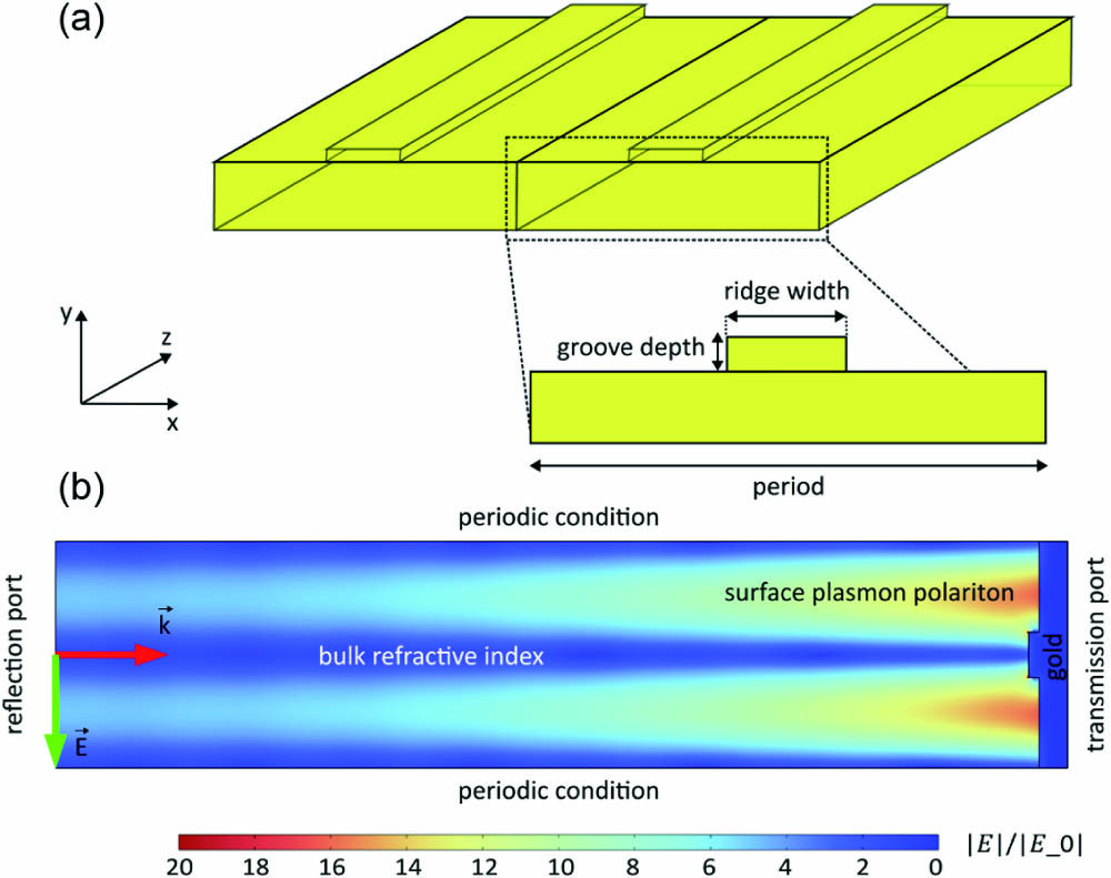
Figure 1.(a) 3D illustration of the gold grating-based SPR sensor with an emphasis on the cross section of a unit cell of the grating (periodicity along
C. Design Process
The grating was initially set with a groove depth of 50 nm and a duty cycle of 0.5, where the duty cycle was defined as the ratio between the ridge width and the period. The grating period was preoptimized by a sweep of the period around the analytical period estimated in Eq. (2) under a normal excitation wavelength of 1550 nm. Once the preoptimal period was determined, we kept it fixed in two separate optimization models, one for the duty cycle and the other for the groove depth at three duty cycles (20%, 50%, and 80%). For each parameter variation, we monitored the SPP coupling efficiency of the sensor. The results gave the trend on the influence of the groove parameters on the FWHM and SPR dip.
As follows from Figs. 2(a) and 2(c), an increase in either the duty cycle or the groove depth resulted in a broadening of the SPR dip. Notably, SPP coupling did not occur when the duty cycle fell below 10% or when the groove depth was less than 10 nm. In Fig. 2(b), a grating with a 20% duty cycle had a narrow and stable FWHM of SPR dip with variations in groove depth. Conversely, in Fig. 2(d), a grating with an 80% duty cycle exhibited significant broadening of the SPR dip at greater groove depth. Based on Fig. 2, a duty cycle of 20% and a groove depth of 55 nm were selected as optimal. This choice ensured that the dimensions of the grating remained comfortably above the fabrication tolerances, on the order of a few tens of nanometers. Finally, the grating with the optimal groove dimensions was further optimized by sweeping the period, aiming to place the SPR dip at the beginning of the tuning range of the laser, i.e., 1532.5 nm. The optimal period was 1160.0 nm.
![]()
Figure 2.Computational SPP coupling efficiency of different grating configurations covered by water (
D. Fabrication
A 4-inch silicon wafer was used as a substrate for SPR sensors. Two sensors were manufactured on the wafer. Sensor 1 has a period of 1160.0 nm, a groove depth of 55 nm, and a duty cycle of 20%. To study SPR mode splitting at different duty cycles, Sensor 2 with a period of 1141.0 nm, a groove depth of 55 nm, and a duty cycle of 50% was fabricated. Each sensor covered an area of . The sensor patterns were fabricated using e-beam lithography and then transferred to a silicon substrate by plasma etching. Subsequently, the silicon master was replicated using nanoimprinting. Finally, replicated patterns were coated with gold by thermal evaporation.
1. E-beam Lithography
A 4-inch silicon wafer was exposed to plasma for 2 min before resist deposition. A layer of diluted negative resist (AZ nLOF 2070, MicroChemicals, Ulm, Germany) was spin-coated (Laurell WS-650MZ-8NPPB, Lansdale, PA, USA) at 4000 r/min for 60 s. The whole wafer was transferred to a 110°C hot plate for a 1 min soft-bake. The predefined grating structure was then written onto the resist layer by electron beam lithography (EBL, Vistec EBPG5000 + HR, Dortmund, Germany). The acceleration voltage was set at 100 kV, and an exposure dose of was used. After exposure, the sample was hard-baked at 110°C for another 1 min. The pattern was then developed in AR 300-47 (AllResist, Strausberg, Germany) for 90 s and then stopped in deionized (DI) water for 60 s before rinsing with DI water.
2. Silicon Master Etching
The grating structure was then transferred to the silicon wafer by inductively coupled plasma-reactive ion etching (ICP-RIE) in the Plasmalab 80Plus system, Oxford. The active gases , , and flowed at the rate of 40, 13, and 2 sccm, respectively, during etching. The chamber pressure was 15 mTorr, while the RIE and IPC powers were set as 40 W and 150 W. The etching time was 40 s. The patterned silicon wafer was used as a master in nanoimprint replication.
3. Anti-adhesion Coating
The silicon master was first coated with an anti-adhesion layer by evaporation of tridecafluoro-(1,1,2,2)-tetrahydrooctyl-trichlorosilane (F13-TCS) [42,43]. Before coating the master was cleaned with acetone followed by DI water rinsing and nitrogen blow drying. The master was then heated on the hot plate for at 150°C to evaporate water residues from the surface. Subsequently the wafer was -plasma treated for 5 min under 0.6 mbar and 200 W (PICO, Diener electronic). The anti-adhesion coating procedure was made in the nitrogen atmosphere in a glove box. A Petri dish with the master inside was placed on a hot plate and ramped from room temperature to 225°C and maintained there for 10 min before applying 40 μL of silane into the Petri dish. After 1 h, the Petri dish with the master was taken out from the glove box. The master was rinsed with acetone, then with DI water, and dried with nitrogen.
4. First-Generation Replication
A 4-inch glass wafer was used as a substrate for first-generation replicates. The cleaning procedure was similar to that of the master. A layer of OrmoPrime08 adhesion promoter was spin-coated at 3000 r/min for 60 s (OPTIcoat SST20+, SSE) on a cleaned glass wafer and baked on the hotplate at 150°C for 5 min. A large drop of OrmoStamp polymer was applied to the center of the master. The glass wafer and the master were then firmly pressed together with the in-house tool in order to obtain sufficiently spread OrmoStamp layer. The OrmoStamp was cured with OmniCure LX400 UV-light source (Lumen Dynamics) for 4 min. The wafer was carefully detached from the master and hard-baked on the hotplate at 230°C for 2 h. The first-generation replicates were coated with an anti-adhesion layer as described above. The only difference in the anti-adhesion coating procedure was the shorter -plasma treatment time (0.3 min instead of 5 min).
5. Second-Generation Replication
A 4-inch silicon wafer was used as a substrate for second-generation replicates. An almost similar fabrication procedure to with the first-generation replicates was used. The only differences were the use of OrmoCore instead of OrmoStamp, and there was no need for an anti-adhesion layer. After the wafer was carefully detached from the first-generation replicate, it was baked at 130°C for 10 min.
6. Gold Deposition
The second-generation replicates were gold-coated using thermal evaporation. We used gold as an SPR-active metal due to its high stability [22]. The replicate was -plasma treated for 24 s and at 200 W (Tepla 440-G, Technics Plasma GmbH). The replicate was placed into the evaporation chamber (MB-20G, Mbraun). The surface was first coated with a 5-nm chromium layer as an adhesive layer. A 150-nm gold layer was then deposited on top of the chromium layer. We chose 150-nm thickness as an optimal due to two reasons. First, the gold thickness needed to be larger than the gold skin depth at 1550 nm, i.e., 30 nm [44]. Second, this choice balanced considerations such as thin-film homogeneity, surface roughness, and slanted profile [45].
7. Characterization
SEM images of the fabricated silicon master and the gold-coated replicate are shown in Fig. 3. The silicon master had fabrication uncertainty below 5 nm in period and ridge width. However, the gold-coated nanoimprinting replicate exhibited variations of a few tens of nanometers compared to the targeted values.
![]()
Figure 3.SEM images of the fabricated silicon masters (left) and the gold-coated replicates (right). (a), (b) Sensor 1 with a designed duty cycle of 20%. The measured duty cycle of gold-coated replicate of Sensor 1 was 25%. (c), (d) Sensor 2 with a designed duty cycle of 50%. The measured duty cycle of gold-coated replicate of Sensor 2 was 52%.
E. Tolerance Analysis
In the design process, the model was simplified by using a bulk gold grating since the gold layer thickness of gold-coated replicates was thick, i.e., 150 nm. In addition, we assumed that the grating had a rectangular profile. However, the fabrication process introduced a slanted profile. In Fig. 4, we modeled the gold-coated replicate with different slanted angles. The model had a patterned polymer layer with an RI of 1.5, a 5-nm chromium layer, and a 150-nm gold layer. In the inset in Fig. 4(a), there was no difference between bulk gold and gold-coated replicate models. Figure 4(a) shows a stable SPP coupling efficiency in slanted gratings. However, there was a slight shift (below 1 nm) in the SPR dip of the slanted gratings. The SPR sensor relies on wavelength shifts, making the influence of the slanted gratings on the SPR measurements essentially negligible. Additionally, we found that the increase in slanted angle broadened the SPR dip [Fig. 4(b)].
![]()
Figure 4.Fabrication tolerance analysis. (a) Computational SPP coupling efficiency of gold-coated replicate with a slanted angle
It is worth noting that writing areas in the EBL process were large, i.e., . This might cause stitching-related issues. However, the diameter of the sensing area was 2.1 mm, which can be considered significantly larger than the stitching-related tolerances. Therefore, we assumed that the stitching issues might have a very limited impact on the performance of the sensor.
3. RESULTS AND DISCUSSION
A. SPR Mode Splitting
Figure 5 shows simulation results of gratings and a groove depth of 50 nm and a varying duty cycle in water under small nonzero incidences (0.1° and 0.3°). Notably, gratings with a duty cycle between 40% and 60% showed a strong SPR mode splitting at nonzero incidences. Gratings with a duty cycle above 60% maintained a stable SPR dip with a slight red shift at 0.3° incidence in comparison with normal incidence in Fig. 2(a). Conversely, gratings with a duty cycle below 30% exhibited a consistently stable SPR dip at 0.1° incidence [Fig. 5(a)] and at normal incidence [Fig. 2(a)]. However, at 0.3° incidence, the SPP coupling on these gratings ceased. Further investigations of SPP coupling at higher incidence angles are presented in Fig. 6. Based on our analysis, one should avoid employing gratings with a duty cycle falling within the 40% to 60% range when configuring the SPR setup for normal incidence. Gratings with a duty cycle below 30% offer two distinct advantages for the normal incidence configuration: a narrow SPR dip and no SPR mode splitting. In this work, we utilized a grating with a duty cycle of 20%.
![]()
Figure 5.Computational SPP coupling efficiency of grating with a groove depth of 50 nm and a varying duty cycle in water (
![]()
Figure 6.Computational SPP coupling efficiency at higher incidence angles on gratings in water (
To validate simulation results presented in Figs. 5 and 6, we constructed a simple experimental setup, which is illustrated in Fig. 7. The light source (HL-2000-HP-FHSA, Ocean Insight, US) injected the light into the input of the reflection/backscatter probes (QR400-7-VIS-NIR, Ocean Insight, US). Light was collimated by a 25-nm lens. The collimated light was polarized by a linear polarizer before hitting the sample. The reflected light was collected by the same probe and analyzed by an NIR spectrometer (NIR Quest+, Ocean Insight, US). To evaluate the resolution of the spectrometer, we analyzed the spectrum of a tunable laser working at 1550 nm. The tunable laser had a tuning resolution of 0.4 nm and a fine-tuning resolution of 0.008 pm. From Fig. 7(b), we found that the used spectrometer had a resolution of 6 nm. We assumed that the nonzero incidence of this setup was below 0.5°. Figure 8 shows the observed SPR mode splitting in the fabricated sensors with different duty cycles. Due to the limited resolution of the used spectrometer (i.e., 6 nm), the SPR dips appeared broader and shallower in comparison with the simulation results. As predicted in Fig. 5, Sensor 2 with a duty cycle of 52% demonstrated a strong SPR mode splitting at nonzero incidence. In contrast, Sensor 1 with a duty cycle of 25% exhibited reduced SPP coupling at nonzero incidence, aligned with the predictions from the simulation.
![]()
Figure 7.(a) Schematic of the optical setup for characterizing the fabricated SPR sensors. (b) Spectrum of the tunable laser operating at 1550-nm wavelength measured by the used NIR spectrometer. The FWHM of the fit curve is 6 nm, which was caused by the spectral resolution of the NIR spectrometer.
![]()
Figure 8.Experimental observation of SPR mode splitting in water (
B. Experimental Setup
A portable experimental setup [Figs. 9(a) and 9(b)] was used to perform SPR measurements. We employed a C-band tunable laser (, TLX1, Benchtop tunable laser source, Thorlabs, Sweden) as a light source. The dimensions of the optical setup were measured as , excluding the tunable laser source. Figure 9(c) illustrates the schematic of the setup. A polarization-maintaining fiber connected to the tunable laser was used to deliver light into the setup. The fiber had an optical isolator to prevent any reflected light back to the source. The injected light was collimated using a fiber collimator (F220FC-1550, Thorlabs, Sweden) before entering a beam splitter cube. The collimated beam with a diameter of 2.1 mm and a full-angle divergence of 0.05° was directed onto the sample via a mirror equipped with two degrees of tilt freedom, ensuring normal incidence adjustment. Reflected light from the sample was collected using a multimode fiber and subsequently detected by an InGaAs photodetector (DET08CFC/M, Thorlabs, Sweden). To align the beam with the fiber, another mirror with two degrees of tilt freedom was placed in the light collection path.
![]()
Figure 9.Experimental setup using a tunable laser at normal incidence. (a) and (b) Top view and side view of the experimental setup, respectively. (c) Schematic of the optical path. (d) Image of the SPR sensor covered with an AR glass on a sample holder.
The SPR sensor in Fig. 9(d) was fixed on a sample holder. The glass cover had a thickness of 1 mm and was coated with anti-reflection (AR) layers on both sides to minimize the interference between the incident light and the reflected light within the sample solution layer and glass cover. To conduct SPR measurements, a 30 μL droplet of sample solution was pipetted on the sensor and subsequently covered with the AR glass. The sample holder was aligned in the setup to ensure the incident light operating at TM mode.
C. SPR Sensor Characterization
Sensor 1 was first characterized with DI water with a refractive index of 1.318 at C-band [41]. SPR measurements were performed by tuning the wavelength of the laser from 1528 nm to 1565 nm with a step of 1 nm. The reflectance spectrum of flat gold was first recorded as a reference. Then the reflectance spectrum from Sensor 1 was measured and divided by the reference spectrum to neglect the water absorption. Figure 10(a) compares the reflectance spectrum of Sensor 1 between simulation and experiment. The experimental SPR dip appeared red shifted in comparison with the simulation due to tolerances in the period, the ridge width, the groove depth, and the slanted profile of fabricated sensors. Since the SPR sensor measures shifts of the resonance wavelength, this red shift did not impact the results. The crucial parameter of interest is the FWHM of the SPR dip. The simulation yielded an FWHM of 2.7 nm, while the experimental FWHM was slightly broader (4.8 nm). This was a result of the slanted profile in fabricated sensors and was in good agreement with the prediction of the 70° slanted angle in Fig. 4(b).
![]()
Figure 10.Characterization of Sensor 1. (a) Comparison between simulation and experiment of reflectance spectrum. (b) Comparison between the simulation and experiment of SPR dip shift as a function of RI change of glucose solution. The labeling value is the mass fraction (in kg/kg). The experimental sensitivity was determined by the slope of the linear fit applied to the experimental data. Each concentration was measured three times.
D. Bulk Refractive Index Sensing of Glucose
Sensor 1 was tested for the detection of changes in bulk RIs of glucose solutions. The glucose solutions were prepared at different concentrations. In Table 1, we measured the RI change of glucose solutions with an Abbe refractometer (ATAGO, DR-M2). It is worth noting that the measured RI changes were at the wavelength of 589 nm. In this work, we employed the C-band. However, the RI change is similar between the visible region and the C-band when the analyte concentrations are changed [41]. Therefore, we can use the values in Table 1 for characterizing Sensor 1 at the C-band. The SPR dips at different concentrations were found by tuning the wavelength from 1528 nm to 1565 nm with a step of 1 nm. For each SPR dip, we conducted a high-resolution tuning step, i.e., 0.25 nm, around the resonance wavelength to precisely locate the characteristic dip of the SPR. The recorded spectra were processed in MATLAB. They were improved by using the smooth function with the moving average method. The SPR dips were determined by finding the minimum value of the spectra using MATLAB functions. There was no need to measure reference spectra from flat gold for three reasons. First, the SPR dip had a notably narrow FWHM. Second, the sensor exhibited strong SPP coupling, resulting in a reflectance of less than 10% at the SPR dip. Third, the impact of water absorption and interferences was minimal compared to the efficiency of SPP coupling. Measured RI Change of Glucose Solutions at 589 nm at Room TemperatureMass Fraction (kg/kg) RI Change 0.00 0.0000 0.05 0.0073 0.10 0.0150 0.15 0.0233
Figure 10(b) shows the shift in SPR dip in the presence of glucose when compared to the SPR dip of DI water (used as a reference). The simulated SPR shifts were calculated by multiplying the simulation sensitivity (1257.5 nm/RIU) with the RI changes in Table 1. The experimental SPR shift exhibited a linear increase as a function of RI change. The sensitivity of the fabricated SPR sensor was 1101.6 nm/RIU, which was determined by the slope of the linear fit applied to the experimental data. In Table 2, we compare the performance of our sensor with some reported grating-based SPR sensors. Notably, the experimental FOM of the sensor was 229.5. The FOM is particularly important at low concentrations where system noises limit detectable SPR shifts [39,48]. The resolution of the SPR sensor was estimated by calculating the ratio between the tuning resolution of the laser and the experimental sensitivity [14], which was on the order of RIU. The estimated RI range of detection was from 1.3180 to 1.3516 at the C-band, which was limited by the tuning range of the laser. Comparison of the Performance of Our Sensor with Other Grating-Based SPR Sensors Reported in the LiteratureReferences Sensitivity (nm/RIU) FOM Resonance Wavelength (nm) Lopez-Munoz 425.0 35.0 525–750 Cao 686.8 21.0 750–800 Long 1477.7 35.2 850–900 Sun 637.0 21.2 650–700 This work 1101.6 229.5 1528–1656
E. Low Concentration Detection
The performance of our SPR sensors in detecting small bulk RI variations was investigated at low concentrations of two analytes, i.e., glucose and creatinine. We tuned the wavelength with a fine resolution of 0.1 nm within a narrow range, i.e., 1533.5–1538.5 nm. The recorded spectra were processed in MATLAB. They were improved by using the smooth function with the moving average method. The SPR dips were determined by finding the minimum value of the spectra using MATLAB functions. Figures 11(a) and 11(b) show the SPR dip as a function of glucose and creatinine concentration. A linear fit was applied to the experimental data to calculate the limit of detection (LoD). LoD is defined as , where is the standard deviation and is the slope of the linear fit [49]. The LoD for the glucose solution was 14.2 mM, (1 mM = 1 mmol/L), whereas, for creatinine, it was 19.1 mM. The uncertainties of SPR measurements can be attributed to several factors. The increase in solution temperature due to water absorption resulted in RI changes [50]. The second factor was the stability of the used tunable laser. In Fig. 12, we characterized the stability of the laser by replacing the SPR sensor with a mirror. We found that there were fluctuations in the intensity. Another factor was the noise from the photodetector. The alignment of the sensor within the setup may also contribute to shift error in the SPR dip.
![]()
Figure 11.Low-concentration detection. Reflectance spectra with a tuning range of 5 nm and a tuning step of 0.1 nm of (a) glucose and (b) creatinine solutions at different low concentrations. SPR dip as a function of the concentration of (c) glucose and (d) creatinine solutions in water. Each concentration was measured three times.
![]()
Figure 12.Tunable laser stability. (a) Tuning range from 1528 nm to 1565 nm with a tuning step of 1 nm. (b) Tuning range from 1533.5 nm to 1538.5 nm with a tuning step of 0.1 nm. The tuning speed was 15 s per wavelength.
4. CONCLUSIONS
We demonstrated the use of a tunable laser in a grating-based SPR system. The SPR sensor was first designed and optimized for maximizing the sensitivity and FOM in COMSOL Multiphysics. The sensor was then fabricated using nanoimprint replication, which is cost-effective for point-of-care applications. In the experimental setup, the usage of a tunable laser made the use of spectral and moving components obsolete, which allows highly integrated systems. Additionally, the setup worked at normal incidence, which is suitable for collinear configuration for compact designs. We demonstrated, both computationally and experimentally, the splitting of the SPR mode at small nonzero incidence, which was lacking in previously reported studies. The fabricated sensor exhibited a high sensitivity of 1101.6 nm/RIU and a remarkably large FOM of 229.5. This was in good agreement with the simulation results. The sensor was characterized in the detection changes in RI in low-concentration solutions of glucose and creatinine. The LoD was 14.2 mM (glucose) and 19.1 mM (creatinine). These results demonstrate the potential of our portable SPR sensor for point-of-care applications.
References
[18] P. Hausler, C. Roth, T. Vitzthumecker. Miniaturized surface plasmon resonance based sensor systems-opportunities and challenges. Photonics and Laser Technology, 223, 169-195(2019).

Set citation alerts for the article
Please enter your email address
© Copyright 2018-2021 | Chinese Laser Press. All Rights Reserved 沪ICP备15018463号-20