
Long Zhang, Xiaolin Yi, Dajian Liu, Shihan Hong, Gaopeng Wang, Hengzhen Cao, Yaocheng Shi, Daoxin Dai. Silicon photonic spectrometer with multiple customized wavelength bands[J]. Photonics Research, 2024, 12(5): 1016
- Photonics Research
- Vol. 12, Issue 5, 1016 (2024)
Abstract
1. INTRODUCTION
Spectrometers have played a pivotal role in both scientific research and daily life, finding diverse applications in fields such as gas sensing, drug analysis, health monitoring, and aerospace exploration [1]. Nevertheless, conventional spectrometers relying on free-space optics are usually cumbersome and expensive. The advent of on-chip spectrometers heralds a transformative era [2], enabling the development of cost-effective and highly portable spectrometers. Silicon photonics, distinguished by the high refractive index contrast and the compatibility with complementary metal-oxide semiconductor (CMOS) processes, provides an attractive option for realizing economical systems-on-a-chip [3]. The spectral resolution and the working window usually are the core indicators for evaluating spectrometers [1], and high resolution and a wide working window are desirable. However, the pursuit of an extremely broad working window and high resolution inevitably leads to many channels with large footprints, high power consumption, low processing yield, and a long scanning time. This is why there is often a trade-off between the working window and the resolution.
Currently there are mainly three kinds of on-chip spectrometers. For dispersion spectrometers [4–8], the key is the dispersive element, such as arrayed waveguide gratings (AWGs) [4], etched diffraction gratings (EDGs) [5], distributed Bragg reflectors (DBRs) [6], and arrayed microrings [7]. For AWG/EDG spectrometers, a large number of channels are usually required to achieve high resolution. For the DBR-based spectrometers shown in Ref. [6], the side-lobe suppression ratio (SLSR) is even as high as due to the undesired side-mode excitation. For the scheme using arrayed microrings, precise alignment of the resonance wavelengths is required for all the microrings in the array, which makes it difficult to guarantee the robustness and the yield. Fourier spectrometers are usually designed with Mach–Zehnder interferometers (MZIs) and are attractive for Fellgett’s advantage [9–12], in which case the bandwidth is limited by the power splitters in the MZIs and the resolution/bandwidth is also dependent on the maximal/minimal optical path difference between the two interference arms. Although various genres have been proposed (including the thermal optics effect [9], digital optical path manipulation [10], MEMS [11], and speckle spectrometers [12]), each presents challenges in the form of intricate calibration processes and limited noise tolerance. More recently, achieving spectral reconstruction with multiple random weakly correlated spectral envelopes in a compact size has attracted intensive attention [13–20]. For example, the tailored disorder modes spectrometer was reported with a resolution of 0.25 nm in a 30 nm wide working window [20], and a dual microcavity spectrometer was demonstrated with a working window of 100 nm [17]. However, this approach is usually very sensitive to fluctuations in the temperature, which poses challenges in real applications. Furthermore, these reconstruction-type spectrometers are predefined and a priori determination for the spectral range to be measured is needed.
Note the fact that it is not always necessary to give the spectral analysis for the whole wavelength span in real applications. Instead, people often pay attention to the spectra for some specific wavelength bands. For instance, in the realm of infrared (IR) spectroscopy and Raman spectroscopy [21], only the specific wavelength bands covering the molecular absorption peaks and the characteristic spectra are of interest, whereas the spectral information in other wavelength bands is deemed irrelevant. Therefore, we propose for the first time, to the best of our knowledge, the concept of a customized on-chip spectrometer by including the specific wavelength bands selected for key application scenarios. With this strategy, the spectrometer design becomes very flexible, so that it not only covers multiple wavelength bands in a very large wavelength span, but also allows high resolution, as demanded for diverse application scenarios.
Sign up for Photonics Research TOC. Get the latest issue of Photonics Research delivered right to you!Sign up now
In this paper, we propose a customized multiband silicon photonic spectrometer by selectively introducing multiple channels of wideband optical filters based on multimode waveguide gratings (MWGs) for pre-filtering and the corresponding thermally tunable narrowband resonators for high resolution. The proposed spectrometer is designed flexibly with the wavelength bands/resolutions as required to satisfy the demands in the real application scenarios, in which way superfluous channels are eliminated to save the space and reduce the configuration complexity as well as the calibration/measurement cost. The MWG-based wideband optical filters are designed optimally with triangular/rectangular teeth to achieve the required wavelength band. The thermally tunable narrowband resonators are designed with a high -factor by introducing broadened microring waveguides to enable high resolution. As an example, we have designed and realized a multiband silicon photonic spectrometer customized with the wavelength bands centered around 1310/1560/1570/1930 nm for sensing multiple gas components like HF, CO, , and . To the best of our knowledge, this is the first on-chip silicon photonic spectrometer available for gas sensing in such an ultralarge wavelength span. In the present case, these four wavelength bands have the desired bandwidths of 6.1/10.3/10.3/10.6 nm, while the corresponding resolutions are 0.11/0.08/0.08/0.37 nm, respectively. For the present spectrometer, the footprint is as compact as and the fabrication process is fully compatible with standard multiproject wafer foundry processes. Such an on-chip spectrometer is expected to potentially play an important role in the applications including gas sensing, aerospace, and portable spectral analysis because of its ultralarge wavelength span, high resolution, compact size, and high design flexibility.
2. PRINCIPLE AND DESIGN
Figures 1(a) and 1(b) show the 3D view and the top view of the present customized multiband silicon photonic spectrometer, which consists of several wideband filters for pre-filtering the specific bands and the corresponding thermally tunable narrowband filters based on high- MRRs in cascade to achieve high resolution. Here we consider the example for sensing multiple gas components, and the principle of spectral analyzing is shown in Fig. 1(c). Here the unknown input spectrum to be measured was pre-filtered into several passbands by the corresponding MWG-based wideband filters, whose transmissions are given by (here ). The prefiltered spectra are then finely filtered by the corresponding thermally tunable high- MRR filters, whose transmissions are given by . Here the -th resonance wavelength is dependent on the heating power , and one has , where is the resonance wavelength when no heating power is applied (i.e., ). As a result, one has the total transmission for the -th output channel of the spectrometer as . In this way, the detected signal at the -th output port is given by
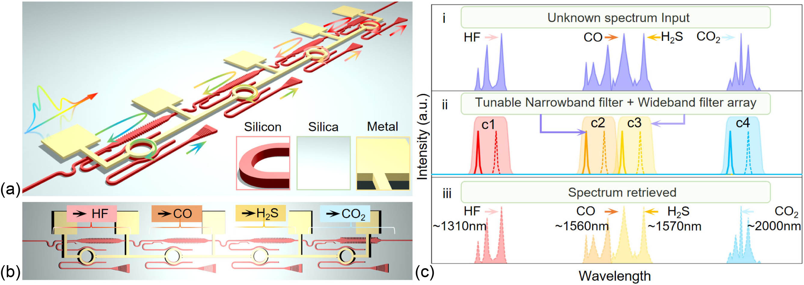
Figure 1.Present silicon photonic spectrometer with multiple customized wavelength bands: (a) 3D view; (b) top view; and (c) the principle.
Note that the transmission acts as the pulse function because of the narrowband response of the high- MRR used. As a result, Eq. (1) can be rewritten as
Finally, the spectrum can be retrieved with the help of the map, i.e.,
For the wideband filters, it is usually desirable to obtain square spectral responses whose central wavelengths and bandwidths can be designed flexibly. Besides, low excess losses and high sidelobe suppression ratios (SLSRs) are also highly demanded. According to our previous works [22,23], here we choose the MWG-based filters, each of which is composed of an apodized MWG and a mode (de)multiplexer based on an adiabatic taper, as shown in Figs. 2(a) and 2(b). Here the MWGs are used to convert the launched mode to the reflected mode in the wavelength band around the Bragg wavelength. The backward mode is then converted to the mode through the mode (de)multiplexer and output at the drop port. Here the phase-matching condition is given as , where and are, respectively, the effective indices of the and modes in the MWG, is the Bragg wavelength, and is the grating period. In this way, the desired spectral band can be efficiently selected to the drop port. To improve the SLSRs, the MWGs are designed with optimal longitudinal apodization [22,23]. For example, the superposition of the gratings is modulated with a Gaussian function along the propagation direction , i.e.,
![]()
Figure 2.(a) Triangular corrugation MWG wideband filter. (b) Rectangular corrugation MWG wideband filter. (c)–(e) Longitudinal apodization for the triangular corrugation MWG. (f)–(h) Longitudinal apodization for the rectangular corrugation MWG. (i) Mode (de)multiplexer based on an adiabatic dual-core taper; and (j) bent coupling based narrowband filter.
In this paper, we developed a multiband silicon photonic spectrometer customized with the wavelength bands centered around 1310/1560/1570/1930 nm for sensing multiple gas components like HF, CO, , and . Regarding the ultralarge wavelength span of the spectrometer, three broadband mode (de)multiplexers are designed for the wavelength bands of 1240–1340 nm, 1500–1600 nm, and 1900–2000 nm, respectively. Table 1 shows all the optimized parameters, and the calculated transmissions of the designed mode (de)multiplexers are illustrated in Figs. 3(a)–3(c). It shows that they all have low excess losses () and low crosstalk () in the corresponding wavelength bands. Notably, even with a waveguide core deviation of , the excess losses and the crosstalk persistently stay below and , respectively. Structural Parameters for TE0/TE1 Mode (De)multiplexer in Different BandsCenter Wavelength 1310 nm 0.45 0.55 0.25 0.18 1.2 0.2 1.2 12 46 10 1550 nm 0.5 0.74 0.28 0.18 1.2 0.2 0.5 19 40 20 1930 nm 0.7 0.90 0.50 0.18 1.2 0.2 0.5 5 35 30
![]()
Figure 3.Calculated wavelength dependence of the designed dual-core adiabatic taper for (a) the 1310 nm wavelength band, (b) the 1550 nm wavelength band, and (c) the 1930 nm wavelength band. Calculated spectral responses of the transmissions at the drop ports for the designed MWGs at the channels of (d) 1310 nm, (e) 1560/1570 nm, and (f) 1930 nm. Calculated spectral responses for the drop/through ports of designed microring resonators at the channels of (g) 1310 nm, (h) 1560/1570 nm, and (i) 1930 nm.
To achieve the central wavelength, the bandwidth, and the rejection ratio as desired for the -th MWG, we carefully choose the grating width (), the corrugation depth (), the apodization strength (), the grating period (), the grating period number (), and the grating period number in the taper sections () as follows: the grating widths , the corrugation depths , the apodization strength , the grating periods ; the period numbers , and the period numbers . Figures 3(d)–3(f) show the calculated spectral responses for all these four channels. As it can be seen, all these channels have box-like responses with low excess losses of less than 0.08 dB and high SLSRs of more than 20 dB, while their bandwidths are customized as 7, 10, 10, and 12 nm, respectively. Furthermore, the variations of the 3-dB bandwidth are less than 1 nm and 2.5 nm, respectively, for the 1310/1550 nm bands and the 1930 nm band, when there is a core width deviation of .
For the narrowband filters based on high- MRRs, it is desirable to have a large FSR to match the corresponding wideband filter. Furthermore, the linewidth should be sufficiently narrow to achieve high spectral resolution. Here, we introduce high- MRRs realized with the optical waveguides that are broadened far beyond the single-mode regime [26,27], where the sidewall scattering loss can be significantly reduced. Meanwhile, the coupling region and the bending sections in the MRRs should be designed carefully to avoid any undesired higher-order mode excitation. Here, a bent directional coupler (DC) is utilized by introducing a narrow bent bus waveguide, as shown in Fig. 2(j). The core widths for the two waveguides of the bent DC are chosen according to the phase-matching condition [28], while the gap width is designed to achieve sufficient coupling. Here, we choose a design with the following parameters: , , , and for the wavelength bands of 1310 nm, 1560–1570 nm, and 1930 nm, and the corresponding power coupling ratios of the mode are 0.02/0.02/0.02/0.06. Figures 3(g)–3(i) show the calculated spectral responses of the designed MRRs for all channels with a propagation loss of 3 dB/cm (which are reasonably estimated according to the measurement results), showing that the FSRs, the excess losses, and the 3 dB bandwidths are 13.4/14.3/15.6 nm, 1/0.7/1 dB, and 0.1/0.1/0.35 nm, respectively. Additionally, when there is a core width variation of , the variations of the FSRs, the excess losses, and the 3 dB bandwidths are, respectively, less than 0.05 nm, 0.04 dB, and 0.03 nm for all the bands of 1310/1550/1930 nm.
3. FABRICATION AND MEASUREMENT
The designed on-chip spectrometer was fabricated by the MPW foundry (Institute of Microelectronics of the Chinese Academy of Sciences, Beijing) using standard processes of UV lithography and inductively coupled plasma dry etching. The spectrometer was made with a top silicon layer with a 220 nm thickness. There is a 1 μm thick silica upper cladding and a 3 μm thick silica buffer layer. Additionally, a 50 nm thick titanium nitride (TiN) heater with a width of 2 μm was fabricated on the top for thermal tuning by using the evaporation process. The smallest features (i.e., the triangular grating period of 253 nm and the rectangular grating gap of 222 nm) of the spectrometer exceed the linewidth requirement of 180 nm, ensuring adequate fabrication. Figure 4 shows the microscope image of the spectrometer. The chip was packaged on a printed circuit board (PCB) through electrical wire bonding. Here, the edge coupler was used for highly-efficient coupling in an ultrabroad wavelength band ranging from 1240 nm to 2000 nm, as shown in Figs. 5(a)–5(c), showing that the coupling losses are , , in the wavelength bands of 1240–1340 nm, 1520–1600 nm, and 1900–2000 nm, respectively.
![]()
Figure 4.Microscope images of the fabricated multiband customized spectrometer.
![]()
Figure 5.Measured spectral responses for the four channels: (a) 1310 nm, (b) 1560 nm/1570 nm, and (c) 1930 nm.
Figures 5(d)–5(f) show the measured transmissions of the wideband filters by using three superluminescent diode (SLD) sources around 1310/1550/1930 nm and an optical spectrum analyzer. These results are normalized with respect to the transmission of an adjacent straight waveguide on the same chip. It can be seen that the central wavelengths, the 3 dB bandwidths, the excess losses, and the SLSRs for these four channels are 1310/1560/1570/1930 nm, 6.1/10.3/10.3/10.6 nm, 2.1/0.9/0.7/1.5 dB, and 25/15/27/21 dB, respectively, which are consistent with the design values. It is worth noting that the SLSR for the 1560 nm band is relatively low, which is due to the imperfect fabrication of the grating teeth.
For the fabricated MRRs working in the four wavelength bands, the spectral responses at the through/drop ports were also characterized, as shown in Figs. 6(a)–6(d). Their 3 dB bandwidths, -factors, and FSRs are 0.11/0.08/0.08/0.37 nm, 11,900/19,500/19,600/5200, and 13.3/14.4/14.4/15.8 nm, respectively. Here, only the resonance peaks for the mode are observed, indicating that there is no higher-order mode excitation in the broadened resonator waveguide with the present design of bent DCs. Meanwhile, their FSRs are much larger than the 3 dB bandwidth of the corresponding MWG-based wideband filters; thus, the crosstalk between the adjacent wavelength bands is suppressed. Figures 6(e)–6(h) show the measured spectral responses of the thermally tunable high- MRRs when operating with different heating powers, and the measured resonance wavelengths are shown in Figs. 6(i)–6(l) as the heating power increases. It can be seen that the thermal tuning efficiencies for the resonance wavelength of the MRRs are 0.30/0.24/0.25/0.22 nm/mW, respectively. Accordingly, one can achieve a wavelength shifting more than an FSR with a heating power less than 70 mW.
![]()
Figure 6.Measured spectral responses at the through/drop ports of the narrowband filters for the four channels: (a) 1310 nm, (b) 1560 nm, (c) 1570 nm, and (d) 1930 nm. The spectral response of the narrowband filters when applying different heating power for the four channels: (e) 1310 nm, (f) 1560 nm, (g) 1570 nm, and (h) 1930 nm. The resonance wavelength as the heating power
For the spectrum analysis, this one-to-one mapping of between the heating power and the resonance peak wavelength of the MRR-based narrowband filter should be accurately established. In the experiment, the heating power is scanned from 0 to 70 mW with a fine step of , which gives a very fine wavelength sampling step better than 0.015 nm. The scanning is powered by a Keithley Sourcemeter 2400 (Tektronix) with time step, and a thermoelectric cooler (TEC) is applied to stabilize the ambient temperature. Figure 7 shows the established mapping of for all MRRs; thus, one can easily infer the peak wavelength at any heating power when scanning. For example, when , as shown in Fig. 7, the peak wavelengths for the four MRRs are 1311.66/1555.96/1570.40/1933.80 nm, respectively.
![]()
Figure 7.Calibrated wavelength power map. The arrow indicates the peak wavelength
The present on-chip spectrometer was then used to analyze various kinds of unknown spectrum. First, the case of a single-peak spectrum is considered and a tunable laser with the wavelengths of 1309.65/1557/1569/1931.94 nm was input as the light source to be measured. The laser linewidths are 3.2 fm, 0.8 fm, 0.8 fm, and 0.31 nm, respectively. Figures 8(a)–8(d) show the retrieved spectra by the present on-chip spectrometer, which agree well with the spectra measured by an OSA with a similar resolution.
![]()
Figure 8.Retrieved spectrum for a given spectrum with a single peak when using the present on-chip spectrometer as well as a commercial OSA: (a) 1309.65 nm, (b) 1557 nm, (c) 1569 nm, and (d) 1931.94 nm. Normalized retrieved spectrum with double-peak input around 1550 nm: (e) (1559.58, 1559.66) nm, (f) (1557.58, 1562.58) nm, (g) (1569.65, 1569.73) nm, and (h) (1567.58, 1572.58) nm. (i) Measured results for the ultrawide window complex spectrum ranging from 1307 nm to 1935 nm.
To characterize the spectrometer resolution, a dual-peak spectrum with a wavelength interval of 0.08 nm in the 1550–1560 nm span was measured. Figures 8(e)–8(h) show the retrieved result when the dual peak wavelengths (, ) are chosen as (1559.58, 1559.66), (1557.58, 1562.58), (1569.65, 1569.73), and (1567.58, 1572.58) nm, respectively. As we can see, these dual peaks can easily be distinguished; there is a slight difference due to the external temperature variation and the wavelength precision of the laser sources. To verify the ability of retrieving complex spectra, an ultrawide window spectrum ranging from 1307 nm to 1935 nm was constructed, as shown in Fig. 8(i). Here, the flat-top spectrum around 1310 nm was generated using a commercial AWG filter, the multipeak envelope in the wavelength band of 1555–1570 nm was provided by a commercial waveshaper filter, and the spectrum with a single peak locating at 1930 nm was supplied by a tunable laser. The measured results shown in Fig. 8(i) have excellent consistency with the spectra obtained using an OSA. It can be seen that the present on-chip spectrometer works well with these multiple wavelength bands as expected.
Furthermore, the present multiband on-chip spectrometer can be further designed flexibly with optimal performances to match the demands in real-world applications. For instance, the resolution can be designed as desired by modifying the -factor of the resonator, while the working window of any channel can be extended greatly by introducing an MWG with a broadened bandwidth that can be as large as [24] and a microresonator with an ultralarge FSR that can be as large as [28]). Moreover, when a further extended window is required, a simple approach is to set up more channels with an adjacent central wavelength. In this way, one can splice the subband spectra measured from these channels together to construct a combined spectrum. For instance, the spectra from the second/third channels can be combined, enabling the working window extended from 10 nm to 20 nm [see the 1555–1575 nm segment in Fig. 8(i)]. It is evident that the present on-chip spectrometer can be developed with high flexibility to satisfy customized requirements for the bandwidth, the resolution, the channel count, and the central wavelength. In future works, sensor experiments will be carried out for various gases to fully demonstrate the potential applications of the proposed spectrometer.
4. CONCLUSION
In summary, we have proposed and experimentally demonstrated a customized multiband silicon photonic spectrometer, which can be designed flexibly with the wavelength bands/resolutions as required to satisfy the demands of real-world application scenarios. The elimination of superfluous channels greatly saves space and significantly reduces the configuration complexity as well as the calibration/measurement cost. Particularly, the customized multiband silicon photonic spectrometer incorporates multiple selective channels of MWG-based wideband optical filters for pre-filtering and thermally tunable high- resonators to achieve high resolution. For example, we demonstrated a multiband silicon photonic spectrometer customized with the wavelength bands centered around 1310/1560/1570/1930 nm for sensing multiple gas components like HF, CO, , and . These four wavelength bands, respectively, have the desired bandwidths of 6.1/10.3/10.3/10.6 nm, and the corresponding resolutions of 0.11/0.08/0.08/0.37 nm. To the best of our knowledge, this is the first on-chip silicon photonic spectrometer available for gas sensing in such an ultralarge wavelength span. Note that the present spectrometer has a footprint as compact as and the fabrication process is fully compatible with standard multiproject wafer foundry processes. In summary, this type of on-chip spectrometer has shown great advantages with an ultralarge wavelength span, a high resolution, a compact size, and high design flexibility. Therefore, it is expected to play an important role in applications including gas sensing, aerospace, and portable spectral analysis.
References
[3] D. Thomson, A. Zilkie, J. E. Bowers. Roadmap on silicon photonics. J. Opt., 18, 073003(2016).
[11] A. Salem, A. Fathy, A. M. Othman. MEMS FTIR parallel spectrometer for non-invasive skin biochemistry analysis. Conference on Lasers and Electro-Optics, AF2Q.7(2021).

Set citation alerts for the article
Please enter your email address
© Copyright 2018-2021 | Chinese Laser Press. All Rights Reserved 沪ICP备15018463号-20