
Xiaohan Jiang, Wanying Liu, Quan Xu, Yuanhao Lang, Yikai Fu, Fan Huang, Haitao Dai, Yanfeng Li, Xueqian Zhang, Jianqiang Gu, Jiaguang Han, Weili Zhang. On-chip terahertz orbital angular momentum demultiplexer[J]. Photonics Research, 2024, 12(5): 1044
- Photonics Research
- Vol. 12, Issue 5, 1044 (2024)
Abstract
1. INTRODUCTION
Nowadays, there is a growing focus on developing mobile networks that operate at higher frequencies, particularly above 100 GHz, to cater to the ever-increasing demand for information traffic in sixth-generation wireless communication systems [1,2]. The terahertz (THz) wave, specifically within the frequency band of 0.1–10 THz, stands out as an unoccupied and unregulated regime that holds promise for enabling data transmission at very high rates, reaching tens and even hundreds of Gbit/s [3]. This potential has led to the emergence of various techniques such as integrated waveguides [4], wave manipulation [5], direct modulation [6], and multiplexing schemes [7], all aimed at ensuring architectural compatibility for high-level protocols and high-capacity communication. One fundamental technology in the field of THz communication is the efficient modulation of THz waves through wavefront engineering, which allows for facilitating their use in data transmission [8]. Multiplexing is particularly valuable for scenarios that demand ultra-high-speed data transmission and high-capacity applications [9,10]. However, the finite nature of frequency and polarization multiplexing poses limitations on the amount of data that can be transmitted.
To overcome this limitation, vortex beams are being explored as an ideal option to enhance the data-carrying capacity. Vortex beams refer to the light where each photon carries orbital angular momentum (OAM). These beams feature a donut-shaped intensity distribution, a helical phase , and unbounded states , where the topological charge can meet the inherent orthogonality to multiplex data streams, is the azimuthal angle, and is the Planck’s constant divided by . The OAM modes can occupy a significantly large mode space, enabling vortex beams with different topological charges to enhance the channel capacity of optical communication [11,12]. Additionally, such beams offer compatibility with conventional techniques such as wavelength-division multiplexing [13] and polarization-division multiplexing [14], making them suitable for deployment in multidimensional THz multiplexing communication systems [15,16].
Benefitting from arrays of subwavelength meta-atoms with meticulous design and appropriate arrangement, metasurfaces can provide complicated and arbitrary wavefront control capability in a compact and multifunction configuration [17–19]. This capability has attracted extensive attention in various fields such as high-speed communication, information encryption, and quantum entanglement [20–23]. Particularly, there has been increasing interest in the multiplexing and detection of OAM modes using ultrathin and planar metasurfaces [24–29], which has shown great potential in advanced compact systems. However, the availability of mode multiplexers in the THz band is currently limited, hindering the development of highly integrated mode division multiplexing (MDM) systems [30,31]. To address this issue, coupling spatial OAM modes into on-chip systems becomes a crucial step toward ultra-compact MDM-based communication [32–34]. Recent advancements in metasurface-based surface plasmon (SP) wave coupling from free-space light have proved various schemes for the detection of physical quantity measurement [35–39] and biochemical sensing [40,41]. Notably, the identification of OAM modes through functional SP devices at dielectric/metal interfaces has garnered significant interest due to their flexibility and compactness [42,43]. However, on-chip OAM demultiplexing in the THz band has not yet been reported, which poses a significant challenge for the development of terminal components required in the MDM-based THz communication.
Sign up for Photonics Research TOC. Get the latest issue of Photonics Research delivered right to you!Sign up now
This study focuses on integrating the scheme of coupling free-space OAM mode into SP modes within an on-chip system operating at THz frequencies. By employing the slit aperture drilled on a metallic film and leveraging its geometric phase, we can identify the OAM of incident circularly polarized vortex beams and guide the coupled SP waves toward predefined directions. We conducted a proof-of-concept experiment, an on-chip OAM mode demultiplexer with seven channels, exhibiting an average isolation level of . Near-field THz scanning microscopy (NTSM) was utilized to characterize the performance of the on-chip OAM demultiplexer directly. The experimental results demonstrated excellent directionality. This compact and realizable on-chip device holds potential for applications in THz mode-division-multiplexing communication and OAM-related information processing.
2. RESULTS
A. Holographic Approach to On-Chip OAM Demultiplexer Design
Here we designed a multichannel demultiplexer for selectively coupling space OAM modes to on-chip SP waves by employing the geometric phase [44,45] and the two-dimensional holographic approach [46,47]. The excited SPs can be steered by rotating a set of subwavelength metallic resonators, where the narrow slits drilled on the metallic film are commonly adopted to generate effective dipole sources. In the case of a circularly polarized normal incidence with the helical phase profile of , the orientation of each meta-atom can be determined by the geometric phase control scheme, based on the relationship of between the geometric phase and the rotation angle of the narrow slits. For simplicity, the basic principle of holography is the reversibility of the light path. As schematically shown in Fig. 1(a), there are OAM modes working for the left circularly polarized (LCP) incidence corresponding to imaginary foci located in the plane, where each imaginary focus can be treated as a point SP source at wavelength , while there are resonators inside a circular region of radius arranged in a square lattice with a subwavelength period of along both the and directions, composing a hologram to record the scattering information from all imaginary foci. The superposition at the th dipole source can be written as
Then the dipole sources emitted from the optimized slit resonators that are drilled on the metallic film are placed at the lattice points with the corresponding rotating angles. As depicted in Fig. 1(b), each dipole source rotated by an angle of with respect to the -axis can only be excited by the incident component polarized along its orientation direction and then produce an SP ripple around in the -plane. Thus, the superposed SP field at an arbitrary point from all the resonators under the LCP incidence can be calculated as
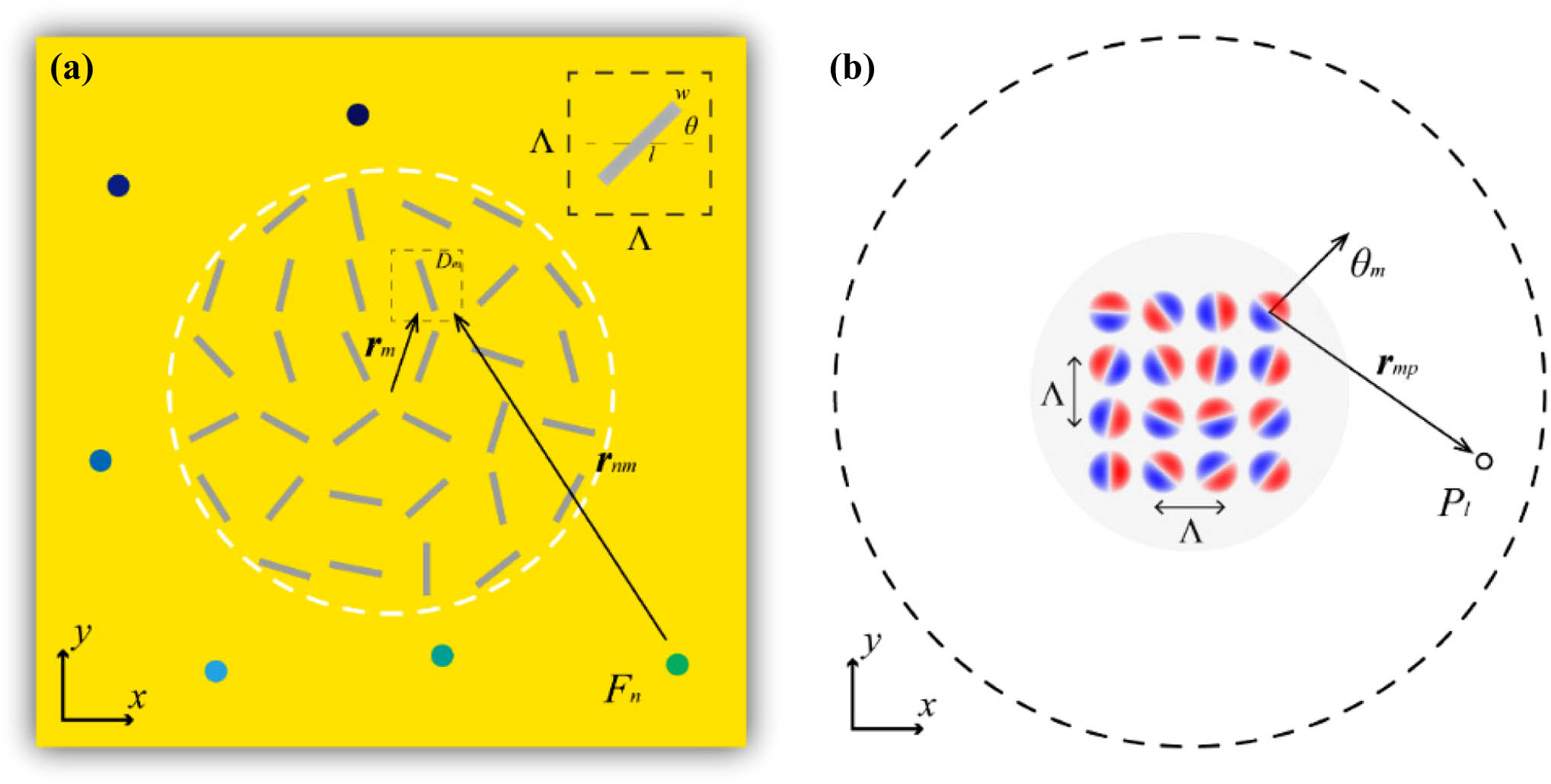
Figure 1.Schematic views of the holographic design scheme for (a) hologram generation and (b) SP field reconstruction. The parameters are:
B. Seven-Channel On-Chip OAM Demultiplexer
Figure 2(a) illustrates a schematic view of a seven-channel vortex-demultiplexing design. Taking advantage of the holographic design principle on a two-dimensional plane, multichannel SP waves coupled from incident vortices will focus to different spots at a radius of 8 mm. The seven focal spots are defined as , , , , , , and , where the twirling colorful rings denoting topological charges of 2, 4, and 6 with the positive sign on the left side and the negative sign on the right will be routed to the corresponding SP focusing directions. The SP beam under the LCP incidence () will be routed to the azimuthal angle of , and the other output channels are arranged with an angle spacing of . The metallic structures of the metasurface containing a total of 5025 slit resonators are periodically arranged with a 100 μm spacing along both the and directions inside a circular region with a radius of 4 mm. The center of the circular region is the origin of the in-plane coordinate system. For simplicity, each imaginary point source is assigned to 1, and the operating frequency is 0.75 THz. In that way, each resonator (70 μm in length and 10 μm in width) is rotated with the specific orientation angle calculated using Eqs. (1) and (2) under the spin direction of LCP, as shown in Fig. 2(b). Such slit structures are fabricated with conventional photolithography and metallization processes (see Appendix A for the details). A portion of the fabricated metallic structures are imaged by a microscope and shown in Fig. 2(c).
![]()
Figure 2.Seven-channel on-chip OAM modes demultiplexing. (a) Schematic of the on-chip demultiplexer design. (b) Calculated distribution of the resonator orientation angles. (c) Microscopy image of the seven-channel OAM demultiplexer.
After the orientation distributions are determined as shown in Fig. 2(b), the numerical results are then calculated using Eq. (3). In the experiment, we obtained the vortex incidences using a series of all-dielectric vortex plates. With the help of the geometric phase in free space, the designed metasurfaces can efficiently convert a Gaussian beam to the vortex beam, and the details can be found in Appendix B. To estimate the performance of these OAM mode convertors, we used NTSM to measure the intensity and phase distributions of the generated vortex beams (see Appendix C for the details), and the measured results are shown in Appendix D. Then the SP fields excited by different vortex beams are mapped by the same THz system. Figure 3(a) exhibits the calculated and measured profiles for OAM incidences with , , , and . The intensity distribution of in each profile is normalized by the corresponding maximum value of intensity, and the fabrication and measurement errors result in the working frequency being shifted to 0.74 THz. Obviously, seven high-quality focused beams propagating respectively along the predefined directions numerically agree well with our proposed design scheme. For detailed analysis among the transmitted channels, the extracted intensities at focal spots are plotted in Fig. 3(b) to show the crosstalk performance, where the focusing intensities are normalized in the same way. Although there exists slight crosstalk in the analysis, the transmitted energies of the SP beams in the target channels can be detected remarkably, indicating low crosstalk and high isolation in the transmission network. The frequency spectra of the corresponding foci are measured and plotted in Fig. 3(c). The average full width at half maximum is 23 μm, which exhibits good quality in terms of both directionality and frequency response.
![]()
Figure 3.Results for the seven-channel OAM demultiplexer. (a) Calculated and measured SP intensity distributions. (b) Extracted intensities at focal spots. (c) Frequency spectra at focal spots.
C. Performance of On-Chip Demultiplexer under Hybrid OAM Mode Incidences
To estimate the performance of the on-chip demultiplexer under hybrid OAM mode incidences, we applied an interleaved method to design multichannel vortex plates to generate multiple OAM modes simultaneously in Appendix E, and the design scheme is the same as that in our previous work [48]. Figures 4(a) and 4(b) are the calculated and measured SP intensity distributions under the incidence of hybrid OAM modes of and . After comparing the calculated results with the measured ones, we deduce that the unwanted noise and crosstalk in the experiment results are mainly caused by the less perfect design and the misalignment of the incidences. Furthermore, as the total incident energy of the THz transmitting antenna remains constant, the intensity of each component in the hybrid OAM modes is halved compared to the case of single mode OAM incidence. This leads to a decrease in the signal-to-noise ratio of the results shown in Fig. 4(b). However, the SP intensity profiles still reflect the function of the on-chip demultiplexer, and the focusing effect can be observed in two directions. The intensity values at the seven focal spots are extracted and shown in Fig. 4(c), in which the results corresponding to and channels are remarkably higher than those of the other channels. As for the incidence of three hybrid OAM modes (, , and 4), the calculated and measured SP intensity distributions, and extracted intensity values at the focal spots are shown in Figs. 4(d)–4(f), respectively. These results further prove that the proposed SP metasurfaces can effectively demultiplex multiple OAM modes, demonstrating the superior performance of our proposed design scheme in on-demand spatial to on-chip OAM coupling and focusing.
![]()
Figure 4.Performance of the on-chip OAM demultiplexer under the incidence of hybrid OAM modes. (a), (d) Calculated demultiplexed SP intensity distributions under the incidence of two and three hybrid OAM modes, respectively. (b), (e) Corresponding measured results. (c), (f) Extracted intensities at focal spots corresponding to the measured results in (b) and (e).
![]()
Figure 5.Generation of incident vortex beams. (a) Schematic of an efficient all-dielectric vortex plate. (b) Microscopy image of a fabricated vortex plate sample (
![]()
Figure 6.Measured intensity (first and third rows) and phase (second and fourth rows) distributions of vortex beams with
![]()
Figure 7.Measured results of vortex beams with hybrid OAM modes. (a), (b) Measured intensity distributions of vortex beams with two hybrid OAM modes of
3. DISCUSSION
Although the proposed device is applied for coupling and focusing vortex beams with specific topological charges of 0, , , and , we can design metasurfaces to demultiplex arbitrary OAM modes based on the holographic method mentioned above. Here, we implement another six-channel demultiplexing with the topological charges of , , and . The schematic of the device and the measured results are shown in Appendix F, indicating the extendibility of our design scheme. Comparing with previous works that have reported on-chip OAM demultiplexing based on a spin-Hall nanograting [42,43], the holographic design has two advantages. One is that propagating directions and focusing spots can be arbitrarily designed; thus SPs can be more flexibly steered on demand. The other is that multidimensional demultiplexing can be further integrated into on-chip devices with the help of the holographic principle, such as wavelength division multiplexing. As shown in Appendix G, we exhibit calculated results of multidimensional demultiplexing for three wavelengths (600 μm, 500 μm, and 400 μm) and three OAM modes ( and ). To implement this multidimensional demultiplexing, a proper resonator with the broadband dipole response in SP excitation needs to be adopted for the design. The results demonstrated in this work exhibit the feasibility of space to on-chip OAM demultiplexing. However, the efficiency of the device should be further improved for practical application. A suggested way to decrease the transmission loss of SP waves is connecting a waveguide after focusing and coupling the beam for postprocessing [49,50], which could be considered in our future work.
![]()
Figure 8.Six-channel on-chip OAM modes demultiplexing. (a) Schematic of the on-chip demultiplexer design. (b) Calculated distribution of the resonator orientation angles. (c) Microscopy image of the six-channel OAM demultiplexer.
![]()
Figure 9.Results for the six-channel OAM demultiplexer. (a) Calculated and measured SP intensity distribution. (b) Extracted intensities at focal spots. (c) Frequency spectra at focal spots.
![]()
Figure 10.Nine-channel on-chip OAM and wavelength demultiplexer. The calculated results are implemented under the incidences of topological charges of
4. CONCLUSION
We proposed and demonstrated a compact strategy for identifying OAM using a flexible geometric-phase-based control approach on a thin metallic film. By adopting the holographic principle, our on-chip multi-channel OAM demultiplexer operates at THz frequencies and can accurately recognize incident circularly polarized waves with any OAM, including those with a topological charge of zero. The coupled SP waves are efficiently routed in different directions, resulting in low crosstalk and high isolation. These superior performance characteristics make our on-chip SP manipulation technology highly advantageous for signal detection and processing in future communication systems. Our SP demultiplexer not only enables the conversion of OAM into on-chip modes in THz mode-division-multiplexing systems, but also contributes to advancements in the design and fabrication of space-to-on-chip couplers. This progress facilitates flexible steering and high-quality focusing of SPs, thereby promoting the development of on-chip information processing and communication.
APPENDIX A: SAMPLE FABRICATION
The on-chip demultiplexer was fabricated using thermal evaporation, photolithography, and metallization processing. First, a 2-mm-thick double-side-polished high-resistance silicon wafer was deposited with 200-nm-thick aluminum using thermal evaporation. Next, a layer of photoresist (AZ P4000) was spin-coated on the aluminum film and subsequently exposed through UV light to pattern the features for OAM demultiplexing in a mask aligner, and then the patterns were revealed after a development process in AZ400K liquid. In the next step, the aluminum in the structure area was removed by etching, and the remaining photoresist was lifted off by acetone, leaving the aluminum film perforated with the structure on the silicon wafer. In addition to the standard steps above, we spin-coated a 10-μm-thick polyimide layer on the fabricated sample to enhance the confinement of the SPs at the metal surface.
APPENDIX B: CONVERTING A GAUSSIAN BEAM TO VORTEX BEAMS
In the last decade, the widespread application of OAM in communications [
APPENDIX C: EXPERIMENTAL SETUP
To experimentally characterize the on-chip OAM-demultiplexing performance, we applied NTSM to directly map the SP fields above the metallic surface. In the experiment, a linearly polarized broadband THz free-space beam was generated from a commercial photoconductive antenna and collimated by a TPX THz lens. Then, a quarter-wave plate was used to convert the linearly polarized beam to a circularly polarized one. After passing through different vortex plates, the beam will carry different topological charges and then be illuminated on the OAM demultiplexers from the substrate side to excite SPs for the demonstration of OAM demultiplexing. It should be noticed that the center of the vortex light must be aligned with that of the sample in the experiment. To avoid this misalignment, we first measured the incident field profiles to determine the centers of incidence. We applied a cage plate mount with the precise removable magnetic plate (Thorlabs, CXY1QF) to make sure of the consistency of the different vortex plates. The sample was finally placed and adjusted under microscopy according to the measured center of light. The SP field was detected by a commercial THz probe that was sensitive to the -polarized electric field component and placed at above the OAM demultiplexers during the measurement.
APPENDIX D: MEASURED ELECTRIC FIELD DISTRIBUTIONS OF GENERATED VORTEX BEAMS
The measured intensity and phase distributions of the vortex beams are shown in Fig.
APPENDIX E: METASURFACE-BASED SIMULTANEOUS GENERATION OF MULTIPLE VORTEX BEAMS
To obtain the incident hybrid OAM modes, we use an interleaved method [
APPENDIX F: SIX-CHANNEL OAM MODES ON-CHIP DEMULTIPLEXING
Taking advantage of the holographic method in Eqs. (
APPENDIX G: CALCULATION RESULTS OF NINE-CHANNEL OAM MODES AND WAVELENGTH DEMULTIPLEXING
Based on the holographic design principle, we proposed a nine-channel demultiplexing scheme. The incident beams include three vortex beams at three wavelengths. The calculated results in Fig.
References

Set citation alerts for the article
Please enter your email address
© Copyright 2018-2021 | Chinese Laser Press. All Rights Reserved 沪ICP备15018463号-20