
Elyes Garoudja, Walid Filali, Slimane Oussalah, Noureddine Sengouga, Mohamed Henini. Comparative study of various methods for extraction of multi- quantum wells Schottky diode parameters[J]. Journal of Semiconductors, 2020, 41(10): 102401
- Journal of Semiconductors
- Vol. 41, Issue 10, 102401 (2020)
Abstract
1. Introduction
The Schottky diode is a microelectronic component based on semiconductor materials. The metallization of this device can give an Ohmic or Schottky contact, according to work function of the used metal. Electrical characterizations of Schottky diode are considered as an important stage before the device final fabrication. Among this electrical characterization, the current voltage (I–V) characteristics are used. Indeed, the extraction of Schottky barrier diodes parameters like ideality factor n, barrier height фb, series resistance Rs and saturation current Is, has attracted the attention of many researchers[
In the literature, the parameters extraction is investigated by using analytical and heuristics technics. The analytical approaches such as Cheung, Werner, and Nord[
Among the proposed works in the literature, the modified ABC algorithm (MABC), vertical optimization, genetic algorithm (GA) and simulated annealing (SA) have been used to extract the SBD parameters[
In this paper, the main contribution is the elaboration of comparative study for different methods of extraction, tested at large range of temperature (from very low temperature 100 K to room temperature 300 K). More precisely, four technics have been developed such as Cheung[
2. Problem statement
2.1. Mathematical model of a Schottky barrier diode
The mathematical model of a Schottky barrier diode (SBD), which is described by its forward bias current, is given by the following expression[
In Eq. (1), Is is the saturation current. The following formula is used to compute its value[
In these equations, I and V are the diode current and bias voltage, respectively. K and A* denote Boltzmann and Richardson constants, respectively; q is the electronic charge; A defines the Schottky contact area; T is the operating temperature. n denotes the diode ideality factor, Rs is the series resistance; and фb is the Schottky barrier height.
2.2. Parameters extraction strategy
The accuracy of the SBD model (given by Eq. (1)) depends on the accurate value of its parameters (more precisely n, Rs and фb). For this purpose, an efficient strategy of SBD parameters extraction has been proposed in this work.
Here, the SBD parameters extraction is considered as an optimization problem, in which the cost criterion to be optimized (in this paper minimized) is the root mean square error (RMSE) between real experimental and estimated Schottky diode currents, as follows:
where
In Eqs. (3) and (4),
L denotes the size of the experimental (I–V) data; Vmeas and Imeas are the measured data gotten from the recorded I–V characteristics.
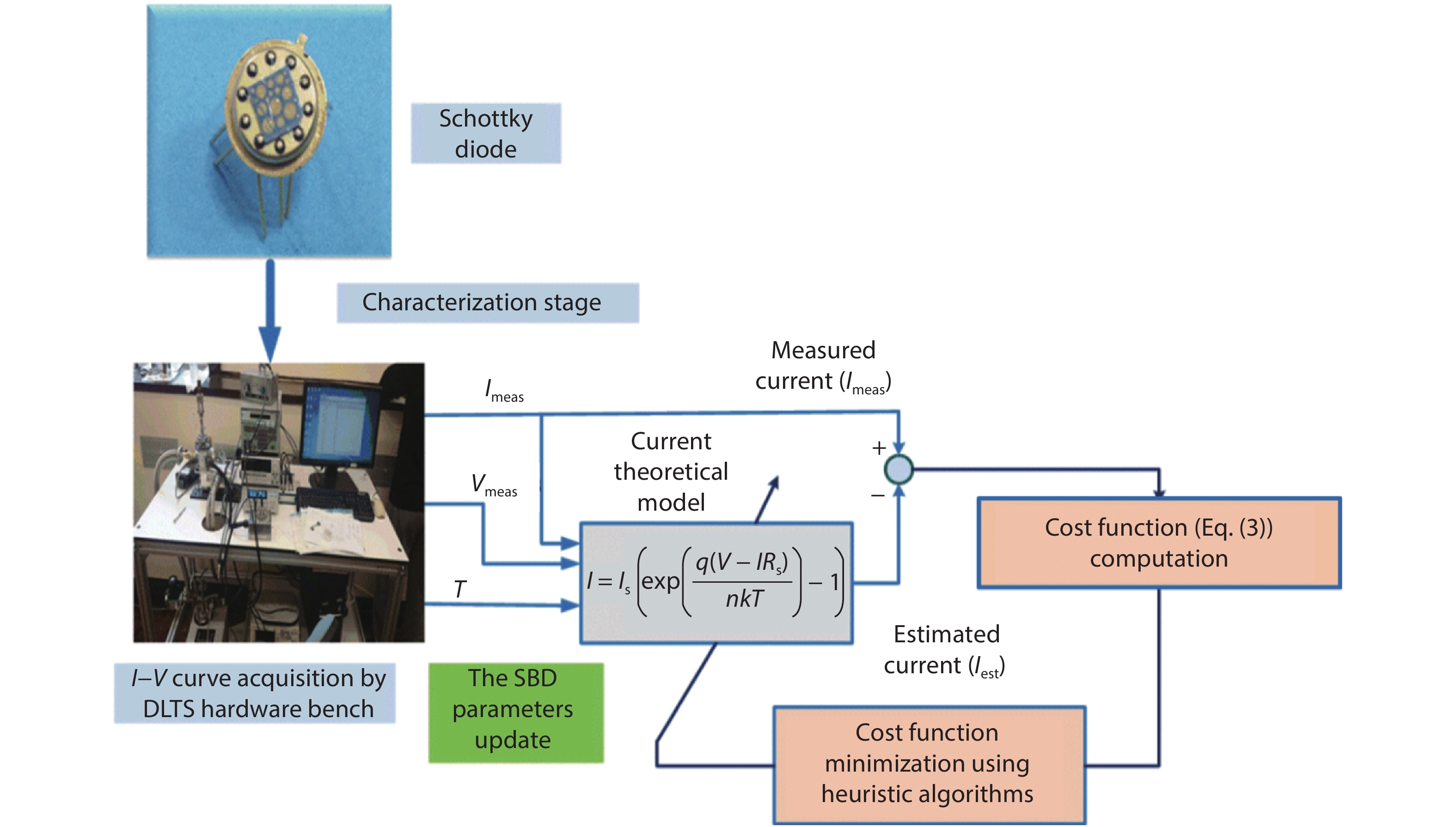
In this paper, the SBD parameters are accurately extracted by using three different heuristics algorithms and an analytical method. Indeed, the heuristic algorithms will change the value of each parameter, in each cycle and within preselected range, until we obtain the lowest cost function (RMSE). Fig. 1 summarizes the main steps of Schottky diode parameters extraction.
![]()
Figure 1.(Color online) The Schottky diode parameters extraction strategy.
3. Experiments
In this work, a multi-quantum wells (MQWs) GaAs/Al0.33Ga0.67As Schottky diode, which was fabricated at Nottingham University (School of Physics and Astronomy Applied)[
The electrical characterization of this diode has been accomplished in the DLTS characterization room of Nottingham University. This room includes the characterization equipment needed to test and characterize electronic components at low/high frequencies and temperatures.
The experimental I–V data of this Schottky diode have been collected and measured by using Agilent 41501B pulse generator and Keithly 428 external I–V meter. The DLTS bench also includes a computer for the DLTS software. The different components of DLTS bench are shown in Fig. 2.
![]()
Figure 2.(Color online) The DLTS characterization bench at Nottingham University.
The experimental (I–V) data have been measured for different temperatures with a sampling rate of 10 ms.
4. Results and discussions
Fig. 3 shows the experimental forward I–V characteristics of the GaAs/Al0.33Ga0.67As Schottky diode. These characteristics were measured at voltage range (0.2–0.7 V) and for low temperature starting from 100 to 300 K. This choice was taken to observe the mechanism of conduction of our sample (Schottky diode) under low temperature conditions (–173 °C).
![]()
Figure 3.(Color online) The
It can be seen from Fig. 3 that by rising temperature, the current value is also increased. This indicates a usual thermal activation phenomenon[
Finally, a comparative study was achieved to evaluate the accuracy of those methods. The setting parameters of those algorithms are given in Table 1. The variation range of the SBD parameters is given in Table 2.
In this simulation, each algorithm was executed 30 times to compute the Mean and STD metrics. Table 3 and Table 4 summarize the obtained parameters for the different competitor methods. These results are the key elements for the comparative study.
From the results of Table 3 and Table 4, the main observation is the large difference of the RMSE values between the heuristics algorithms and the analytical method. So, the analytical method is not a good candidate to solve this problem. Fig. 4 and Fig. 5 show the weakness of Cheung method to extract the SBD parameters against DE algorithm, at 100 and 300 K, respectively.
![]()
Figure 4.(Color online) Experimental and simulated
![]()
Figure 5.(Color online) Experimental and simulated
Our analysis of the results of the algorithms shows that all of these methods are adequate solutions for this problematic. Moreover, the DE algorithm gives accurate parameters (n, Rs, Is, фb) along the entire temperature range, compared with the others. This accuracy is due to the ability of the DE to converge to the lowest RMSE.
Additionally, the robustness of DE algorithm is verified by comparing the STD metric for the three heuristic algorithms. Indeed, STD values of DE are in scale of 10–22, while are in 10–7 and 10–8 for the others.
Fig. 6 shows the convergence rate of DE, PSO and ABC algorithms at T = 100 K. This figure indicates that ABC algorithm presents a rapid convergence till cycle #800. Up to this cycle, ABC algorithm shows slow convergence. The optimal solution was achieved at iteration #4700. In contrast to ABC algorithm, the others show an apparent rapid convergence speed. Where, it significantly increases in case of DE algorithm compared with PSO and ABC.
![]()
Figure 6.(Color online) Convergence characteristics of DE, PSO and ABC algorithms for
The variation of RMSE at each running cycle for DE, PSO and ABC algorithm for T = 100 K is shown in Fig. 7. By analyzing the results in this figure, we can see that by increasing the number of running cycle (30) for the different algorithms, the DE algorithm shows the best robustness. In fact, its RMSE value does not change at almost all running cycles compared with PSO and ABC. Consequently, the SBD parameters do not change.
![]()
Figure 7.(Color online) Variation of RMSE at each running cycle for DE, PSO and ABC algorithm for
5. Conclusion
In this paper, a comparative study was elaborated for different extraction methods. This comparison is divided on two sections; first, the performance of heuristics algorithms was compared with those of analytical method (Cheung method); and second, the efficiency of DE, PSO and ABC algorithms was investigated.
The obtained results show that the performance metrics, convergence rate speed and the accuracy of the parameters determined by the DE algorithm are better than ABC, PSO and Cheung method. In addition, DE is more robust than the other algorithms. As a result, DE is an effective, robust and fast approach for the parameter extraction of the Schottky diode.
References
[1] S Cheung, N Cheung. Extraction of Schottky diode parameters from forward current–voltage characteristics. Appl Phys Lett, 49, 85(1986).
[2] J H Werner. Schottky barrier and pn-junction
[3] Ş Karataş, Ş Altındal. Temperature dependence of barrier heights of Au/n-type GaAs Schottky diodes. Solid-State Electron, 49, 1052(2005).
[4] İ Dökme, Ş Altindal, M M Bülbül. The barrier height inhomogeneity in Al/p-Si Schottky barrier diodes with native insulator layer. Appl Surf Sci, 252, 7749(2006).
[5] N Karaboga, S Kockanat, H Dogan. Parameter determination of the schottky barrier diode using by artificial bee colony algorithm. International Symposium on Innovations in Intelligent Systems and Applications, 6(2011).
[6] A Sellai, Z Ouennoughi. Extraction of illuminated solar cell and Schottky diode parameters using a genetic algorithm. Int J Mod Phys C, 16, 1043(2005).
[7] J H Werner, H H Güttler. Barrier inhomogeneities at Schottky contacts. J Appl Phys, 69, 1522(1991).
[8] H Norde. A modified forward
[9]
[10]
[11] K Wang, M Ye. Parameter determination of Schottky-barrier diode model using differential evolution. Solid-State Electron, 53, 234(2009).
[12] J Kennedy. Particle swarm optimization. Encyclopedia of Machine Learning, 760(2010).
[13]
[14]
[15]
[16] W Filali, N Sengouga, S Oussalah et al. Characterisation of temperature dependent parameters of multi-quantum well (MQW) Ti/Au/n-AlGaAs/n-GaAs/n-AlGaAs Schottky diodes. Superlattices Microstruct, 111, 1010(2017).
[17]
[18]


Set citation alerts for the article
Please enter your email address

© Copyright 2018-2021 | Chinese Laser Press. All Rights Reserved 沪ICP备15018463号-20