Zili Li, Xiaohua Hu, Shisheng Xiong. DSA in Combination with DUV Lithography for Sub-10 nm Manufacturing[J]. Laser & Optoelectronics Progress, 2022, 59(9): 0922027
Search by keywords or author
- Laser & Optoelectronics Progress
- Vol. 59, Issue 9, 0922027 (2022)
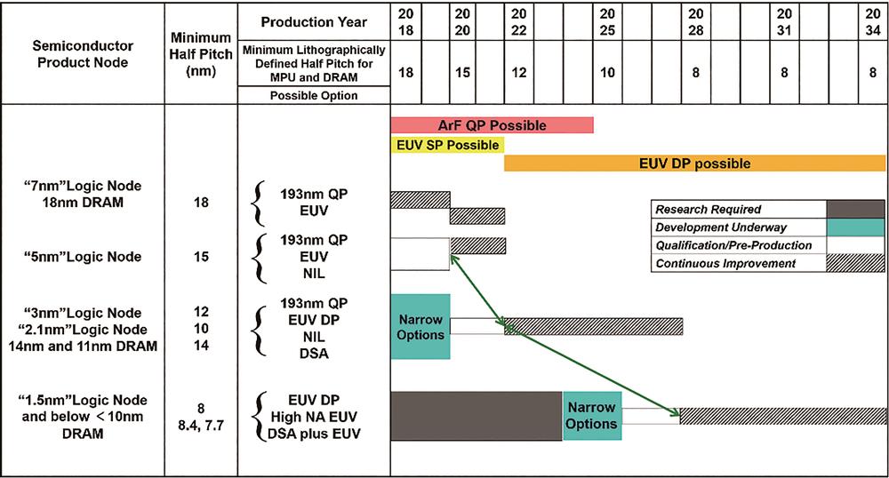
![IRDS advanced technology node development roadmap[11]](/richHtml/lop/2022/59/9/0922027/img_01.jpg)
Fig. 1. IRDS advanced technology node development roadmap[11]
![Schematic and corresponding SEM images of block copolymer-directed self-assembly based on chemical epitaxy and physical epitaxy [17]](/richHtml/lop/2022/59/9/0922027/img_02.jpg)
Fig. 2. Schematic and corresponding SEM images of block copolymer-directed self-assembly based on chemical epitaxy and physical epitaxy [17]
Fig. 3. DSA of layered phase PS-b-PMMA in guiding templates modified by different random copolymers. (a) Schematic diagram; (b) corresponding SEM images[33]
Fig. 4. Schematic diagram and corresponding SEM images of block copolymer-directed self-assembly prepared by physical epitaxy based on 193 nm exposure [34]
Fig. 5. Schematic of DSA lithography technology based on “LiNe flow” method [37]
Fig. 6. Influence of exposure dose on pattern quality before and after transfer in wet etching process with acetic acid as developer and SEM images corresponding to different exposure doses [48]
Fig. 7. Schematic of the self-aligned pre-patterning process route. (a) Chemical guiding pattern; (b) DSA process; (c) O2 etching process; (d) SEM image of pattern transfer process and corresponding process [56]
Fig. 8. Types of patterns required for chip design and patterns demonstrated by DSA lithography [59]
Fig. 9. Evolution of defect density in DSA lithography process [69]
Fig. 10. Self-healing capability of DSA lithography for defects of templates[71]
Fig. 11. Comparison of production costs and processing steps of DSA and SAQP Baseline[20]
Fig. 12. Parameter index spider charts for different lithography techniques [16]
Fig. 13. Schematic diagram of different fabrication stages of FinFET devices based on DSA lithography[20]. (a) Cross-sectional image of etched Si fins; (b) customized fins filled with isolation oxide; (c) dummy gate formation; (d) SEM image of merged source and drain; (e) dummy gate removal and channel exposure; (f) schematic of corresponding three-dimensional structures
| |||||||||||||||||||||||||||||||||||||||||||||||
Table 1. Chip manufacturing technology nodes of different semiconductor manufacturers andtheir corresponding pattern sizes
| |||||||||||||||||||||||||||||||||||
Table 2. Performances and parameters of various lithography techniques[16]

Set citation alerts for the article
Please enter your email address


