• Chinese Optics Letters
  • Vol. 20, Issue 3, 031302 (2022)
Liping Zhou1、2, Chengli Wang1、2, Ailun Yi1、3, Chen Shen1, Yifan Zhu1、2, Kai Huang1, Min Zhou1, Jiaxiang Zhang1、2、*, and Xin Ou1、2、**
Author Affiliations
  • 1State Key Laboratory of Functional Materials for Informatics, Shanghai Institute of Microsystem and Information Technology, Chinese Academy of Sciences, Shanghai 200050, China
  • 2Center of Materials Science and Optoelectronics Engineering, University of Chinese Academy of Sciences, Beijing 100049, China
  • 3XOI Technology Co., Ltd., Shanghai 201899, China
  • show less
    DOI: 10.3788/COL202220.031302 Cite this Article Set citation alerts
    Liping Zhou, Chengli Wang, Ailun Yi, Chen Shen, Yifan Zhu, Kai Huang, Min Zhou, Jiaxiang Zhang, Xin Ou. Photonic crystal nanobeam cavities based on 4H-silicon carbide on insulator[J]. Chinese Optics Letters, 2022, 20(3): 031302 Copy Citation Text show less

    Abstract

    The 4H-silicon carbide on insulator (4H-SiCOI) has recently emerged as an attractive material platform for integrated photonics due to its excellent quantum and nonlinear optical properties. Here, we experimentally realize one-dimensional photonic crystal nanobeam cavities on the ion-cutting 4H-SiCOI platform. The cavities exhibit quality factors up to 6.1×10³ and mode volumes down to 0.63 × (λ/n)3 in the visible and near-infrared wavelength range. Moreover, by changing the excitation laser power, the fundamental transverse-electric mode can be dynamically tuned by 0.6 nm with a tuning rate of 33.5 pm/mW. The demonstrated devices offer the promise of an appealing microcavity system for interfacing the optically addressable spin defects in 4H-SiC.

    1. Introduction

    Silicon carbide (SiC), especially the 4H polytype, is a promising platform for realizing large-scale integrated photonics owing to its prominent material properties, such as high refractive index (2.6 at the C-band), large transparent window, high second- and third-order optical nonlinearities[15], and compatibility with industry fabrication processes. In addition, 4H-SiC can host various optically addressable spin defects[6,7], which work in the visible and near-infrared spectral region. Many of them have proven to be outstanding quantum light emitters with bright single photon emission[8] and long spin coherence time[9]. The available intrinsic spin hosts and quantum light emitters, combined with its favorable material properties, make the 4H-SiC platform a real contender for the realization of large-scale optical quantum circuits[10,11].

    A central challenge of 4H-SiC for spin-based quantum information applications lies in the ability to efficiently extract photoluminescence (PL) emitted by the optically addressable spin defects and to simultaneously engineer the two-level solid-state quantum emitters with a high fidelity[1215]. A long-proposed solution to solve the above challenges is to couple the spin defects with optical microcavities. While many solutions exist, the photonic crystal (PhC) cavity[1621] that is capable of confining light in an extremely small mode volume is an ideal candidate. Recently, two independent research groups have successfully achieved an enhanced light extraction efficiency of the silicon-related defects by employing a PhC nanobeam cavity in 4H-SiC. Despite the advance, their achievements were demonstrated on bulk 4H-SiC and 4H-SiC slab, which were prepared by complex carving[19] and mechanical thinning techniques[10]. Such complexity imposes a limitation to the device functionality and versatility, which renders the practical applications in large-scale integrated photonic circuits inconvenient. A tried-and-true solution to overcome the complex carving technique in bulk material is to employ thin-film 4H-SiC on insulator (4H-SiCOI) prepared by the ion-cutting technique. As compared to the bulk counterpart, the fabrication of the ion-cutting 4H-SiCOI is compatible with the mature CMOS technologies, thus allowing for mass production of a wafer-scale substrate that is essential for large-scale integrated photonic applications[22]. Thus far, tremendous efforts have been made in the development of optical microcavities[4,23,24] on the ion-cutting 4H-SiCOI platform. However, a one-dimensional (1D) PhC nanobeam cavity with sufficiently small mode volume to interface the optically addressable spin defects has not been demonstrated on the ion-cutting 4H-SiCOI platform yet.

    In this work, we design and fabricate 1D-PhC cavities on a 4H-SiCOI platform prepared by the ion-cutting method. We characterize the fabricated PhC cavities using a room temperature PL experiment. The measured PL spectra unveil that the nanophotonic cavities supported transverse-electric (TE)-like modes. The fundamental TE (TE0) mode shows the quality (Q) factor up to 6.1×10³ and a small effective optical mode volume of 0.63×(λ/n)3 in the visible and near-infrared range, making them a promising candidate for applications in cavity electrodynamics and integrated quantum photonic circuits.

    2. Device Design and Fabrication

    The 4H-SiCOI used in this work was prepared by the ion-cutting technique, together with a direct wafer bonding technique. The detailed fabrication process is depicted elsewhere[17] and has proven efficient to provide large-scale 4H-SiCOI with accurately controlled uniformity. First, a 4 in. (1 in. = 2.54 cm) bulk SiC wafer was implanted by H ions with a dose energy of 170 keV, and the ion-induced defects occurred at about 1.1 µm away from the top SiC surface. Then, the implanted SiC wafer was bonded onto a silicon substrate with a 3 µm thick silicon dioxide layer. After annealing at about 850°C, the implanted 4H-SiC thin film was subsequently transferred to the silicon substrate, resulting in the formation of a 4H-SiC thin film on the SiO2/Si substrate, the so-called 4H-SiCOI. Before processing the device, we further thinned down the 4H-SiC thin film to the nanometer scale by employing an inductively coupled plasma (ICP), followed by surface polishing via a chemical mechanical polishing (CMP) technique. The final SiC film thickness and roughness were examined through white light interferometer and atomic force microscopy (AFM), respectively, which yielded a thickness of 280 nm and roughness below 0.3 nm for the thin-film 4H-SiC used in our work.

    As for the device processing, an 800 nm thick H silsesquioxane (HSQ) resist was spin-coated on top of the 4H-SiCOI substrate, and the PhC nanobeam patterns were defined via an electron-beam lithography (EBL) process. The patterns were then transferred to the 4H-SiC film via ICP etching with
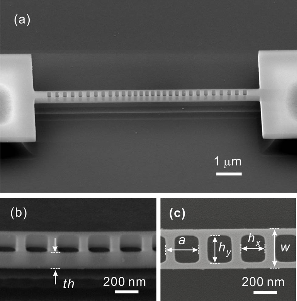
 SF6/O2 plasma. It should be noted that the etching depth exceeds the thickness of the 4H-SiC thin film (280 nm), and therefore the PhC nanobeam cavities can be suspended by etching the lower SiO2 with 10% hydrofluoric acid solution. Meanwhile, the residual HSQ resist was completely dissolved during the undercutting process. Figure 1(a) shows a scanning electron microscope (SEM) image of the fabricated PhC cavity. The total length of the nanobeam cavity is about 10 µm. The geometry of the cavity comprises periodically arranged rectangular air-holes at both ends, which act as two highly reflective mirrors for electromagnetic waves. To form an optical cavity with well-localized optical modes in the axial direction[25,26], we introduce a “defect region” at the center of the nanobeam by quadratically decreasing the lattice constant from a to 80% of a. The resonance wavelength mainly depends on the lattice constant (a) and slightly decreases with the increasing hole length (hx) and width (hy).

    (a) Scanning electron microscope image of a suspended 1D nanobeam PhC cavity. (b) Zoom-in side view image of the PhC cavity, where th is the slab thickness. (c) Zoom-in top view image of the 1D-PhC cavity. The nominal unit cell is parameterized by a (lattice constant, hole to hole distance), w (beam width), hx (air hole length), and hy(air hole width).

    Figure 1.(a) Scanning electron microscope image of a suspended 1D nanobeam PhC cavity. (b) Zoom-in side view image of the PhC cavity, where th is the slab thickness. (c) Zoom-in top view image of the 1D-PhC cavity. The nominal unit cell is parameterized by a (lattice constant, hole to hole distance), w (beam width), hx (air hole length), and hy(air hole width).

    3. Result and Simulation

    To characterize the resonance properties of the fabricated 1D-PhC cavities, we measured the PL spectra of the devices at room temperature using a home-built µ-PL setup, as depicted in the previous work[23]. A continuous green laser (532 nm) was used as the excitation laser and was focused at the nanobeam center. The PL signal was collected by a near-infrared-infinity corrected objective (Mitutoyo NIR 50×). It was then transmitted through a dichroic mirror and collected by a single mode fiber. The PL signal was analyzed by a high-resolution spectrometer (SP-2750) equipped with a thermoelectric-cooled silicon charge-coupled device (CCD).

    An experimental PL spectrum of the PhC nanobeam cavity is shown (blue line) in Fig. 2(a). The broad emission background is likely attributed to lattice imperfections and oxygen-related surface defects introduced by the proton implantation and device fabrication process, which was extensively observed in SiC PL measurement[2729]. In the experimental spectrum, a series of TE-like modes and transverse-magnetic (TM)-like modes are observed. The fundamental, second-, and third-order TE-like modes, denoted as TE0, TE1, and TE2, are located at 825.1 nm, 871.6 nm, and 919.6 nm, respectively. To identify these resonant peaks in the PL spectrum, we employ a three-dimensional (3D) finite-difference time-domain (FDTD) method. The geometric parameters of the cavity are extracted from an SEM measurement, which gives the slab thickness (th) of 280 nm, beam width (w) of 400 nm, lattice constant (a) of 290 nm, and rectangular hole size (hx×hy) of 160nm×285nm. Since 4H-SiC has a hexagonal crystal structure (6 mm point group), its optical anisotropy plays an important role in determining the cavity performance. To take this effect into account, we include the ordinary refractive index (no) and the extraordinary refractive index (ne) described by the Sellmeier equation[30] in our simulations. The purple line in Fig. 2(a) shows the simulated spectrum. The good agreement between the simulated and experimental resonant peaks confirms our mode assignments. We also take a 3D finite-element-method (FEM) simulation to confirm the results above, and the electric field profiles (Ey component) of TE-like modes are shown in Figs. 2(b)2(d). Aside from TE-like modes, TM-like modes are observed in the shorter wavelength range with weak intensity. The 3D FEM simulations show that these TM-like modes have bigger mode volumes and larger scattering losses than the TE-like modes, and thus they prefer to form weaker resonances. Besides, an unidentified optical mode appears between the TE1 and TE2 modes but is not found in the experimental spectrum of another cavity with the same parameters. Although the origin of this mode is not clear at this moment and it occurs possibly due to the Fabry‒Perot resonance between the nanobeam and the silicon substrate, or the travelling mode in the nanobeam reflected by the pad on both sides, the underlying mechanism could be further understood by enhancing the signal-to-noise ratio of the spectrum through increasing the thickness of the buried oxidation layer and the length of the nanobeam.

    (a) Experimentally measured PL spectrum (blue line) and 3D-FDTD simulation spectrum (purple line) from a PhC with a lattice constant of 290 nm. Resonance peaks in the simulated spectrum show a good consistence with the experimental results at room temperature, especially the TE-like polarized modes. (b)–(d) 3D finite-element-method (FEM) simulated optical profiles (Ey component) of the (b) TE0, (c) TE1, and (d) TE2 modes.

    Figure 2.(a) Experimentally measured PL spectrum (blue line) and 3D-FDTD simulation spectrum (purple line) from a PhC with a lattice constant of 290 nm. Resonance peaks in the simulated spectrum show a good consistence with the experimental results at room temperature, especially the TE-like polarized modes. (b)–(d) 3D finite-element-method (FEM) simulated optical profiles (Ey component) of the (b) TE0, (c) TE1, and (d) TE2 modes.

    Next, we characterize the geometry-dependent cavity properties. Figure 3(a) shows the normalized PL spectra of the cavities with different lattice constants. The fundamental TE0 modes are preferentially supported by the PhC nanobeam cavity and have stronger resonant peaks as compared to the high-order TE-like modes. To further quantify the mode properties, we theoretically fit the resonant peaks of TE-like modes with a Lorentz peak function. The PhC cavity with a=270nm exhibits a Q-factor of 2.8×10³, while the PhC cavity with a=290nm exhibits a much higher Q-factor of 6.2×10³. The high Q-factor of 6.2×10³ obtained in our work is on a par with the previously reported nanobeam cavities fabricated with bulk 4H-SiC material[19,31].

    (a) PL spectra of 1D-PhC cavities with lattice constants of 270 nm and 290 nm. The fundamental TE-like modes are located at 753.8 nm and 825.4 nm, respectively. (b), (c) Normalized PL spectra and theoretical fitting (red lines) of the TE0 modes for cavities with lattice constants of (b) 270 nm and (c) 290 nm.

    Figure 3.(a) PL spectra of 1D-PhC cavities with lattice constants of 270 nm and 290 nm. The fundamental TE-like modes are located at 753.8 nm and 825.4 nm, respectively. (b), (c) Normalized PL spectra and theoretical fitting (red lines) of the TE0 modes for cavities with lattice constants of (b) 270 nm and (c) 290 nm.

    In addition, we evaluate another critical parameter of the PhC cavities, i.e., the mode volume (V). It can be defined by the equation[26,32]V0=[ε(r)|E(r)|max(ε(r)|E(r)|)]2dV,where ε(r) is the dielectric constant, E(r) is the electric field profile, and r is the position vector. The TE0, TE1, and TE2 modes of the PhC cavity with a=290nm have a calculated effective mode volume of 0.63×(λ/n)3, 0.89×(λ/n)3, and 0.96×(λ/n)3, respectively. The mode volumes can be less than one cubic wavelength, and therefore these PhC nanobeam cavities are envisaged to provide a tight confinement for light fields at the center of the nanobeam so as to achieve an enhanced light–matter interaction at the sub-wavelength scale. When considering the coupling of spin defects with these nanobeam cavities in 4H-SiC, a Purcell enhancement can be expected, and the Purcell factor can be evaluated by[33]F=34π2(λn)3QV0.

    Given the calculated mode volume V=0.63×(λ/n)3 and measured Q=6.1×10³, the Purcell factor is calculated to be 740. The Q/V ratio is much larger than the whispering gallery mode (WGM) resonators on 3C-SiC material platform[27,34] and comparable with the PhC cavities in crystalline bulk SiC[19]. This prominent enhancement allows for the realization of a spin defect-cavity system, which is an essential step to acquire enhancing light emission and further quantum information processing on the SiCOI integration platform.

    In order to overcome inherent variations of the resonant wavelengths and the inhomogeneous broadening of the spin defects in 4H-SiC, a critical step for realizing an efficient cavity-defect system will be the demonstration of spectral tuning of cavity modes. So far, various techniques such as cryogenic gas condensation[10] and laser-assisted oxidation[35] have been explored. We show here that the cavity modes can be tuned by changing the excitation power. As shown in Fig. 4(a), the power-dependent PL spectra indicate that the peak positions of TE-like modes for the cavity with a=290nm can be dynamically shifted with the excitation laser power. This phenomenon can be interpreted by the intrinsic thermo-optic effect of the 4H-SiC material[36,37]. Specifically, when the excitation laser is focused at the center of the nanobeam, the self-heating effect takes place, which modifies the cavity temperature and, consequently, shifts the cavity resonant positions. The shift efficiency of the TE0 mode can be fitted with a quadratic function, which yields a tuning rate of about 33.5 pm/mW. Similarly, the TE2 and TE3 modes can be red shifted in the same manner, as shown in Fig. 4(b). A different tuning rate is found, and this difference is ascribed to the big discrepancies of the mode volumes for different modes. A more compact mode leads to stronger self-heating effect. Interestingly, we find that the Q-factor of the TE0 mode remains at the value of 6×10³ without measurable degradation as with the increasing excitation power. This characteristic, that is, the cavity mode tunes with the change of excitation power, could be leveraged as an effective means to realize the tunability of PhC nanobeam cavity modes.

    (a) Measured PL spectra as a function of the excitation power. (b) Resonance shift of the TE-like modes (rectangle for TE0, circle for TE2, triangle for TE3) as a function of excitation power.

    Figure 4.(a) Measured PL spectra as a function of the excitation power. (b) Resonance shift of the TE-like modes (rectangle for TE0, circle for TE2, triangle for TE3) as a function of excitation power.

    4. Conclusion

    In conclusion, we have demonstrated 1D-PhC nanobeam cavities on an ion-cutting 4H-SiCOI platform. The cavity modes are located in the visible and near-infrared wavelength range. The cavity shows experimental Q-factors up to 6.1×10³ and mode volumes down to 0.63×(λ/n)3, corresponding to a Purcell factor of about 740. We believe that the Q-factor can be further improved by reducing the scattering and radiation losses using an optimal etching process and cavity geometry. Furthermore, the cavity mode wavelength can be dynamically shifted by changing the excitation power with a tuning rate of 33.5 pm/mW for the fundamental TE mode. Going forward, to achieve the coupling between the presented cavity and the color center, we will continue to optimize our fabrication processes to create higher Q 4H-SiC thin films and develop the ion implantation methods. Moreover, the tuning methods of the cavity mode, such as excitation power tuning reported here and cryogenic gas condensation[38], need to be applied to our nanobeam cavities. With the progress of this work, the nanobeam cavities demonstrated here are expected to accelerate the development of the 4H-SiCOI platform in integrated quantum photonics.

    References

    [1] B.-S. Song, T. Asano, S. Jeon, H. Kim, C. Chen, D. D. Kang, S. Noda. Ultrahigh-Q photonic crystal nanocavities based on 4H silicon carbide. Optica, 6, 991(2019).

    [2] C. Wang, Z. Fang, A. Yi, B. Yang, Z. Wang, L. Zhou, C. Shen, Y. Zhu, Y. Zhou, R. Bao, Z. Li, Y. Chen, K. Huang, J. Zhang, Y. Cheng, X. Ou. High-Q microresonators on 4H-silicon-carbide-on-insulator platform for nonlinear photonics. Light Sci. Appl., 10, 139(2021).

    [3] H. Sato, M. Abe, I. Shoji, J. Suda, T. Kondo. Accurate measurements of second-order nonlinear optical coefficients of 6H and 4H silicon carbide. J. Opt. Soc. Am. B, 26, 1892(2009).

    [4] Y. Zheng, M. Pu, A. Yi, X. Ou, H. Ou. 4H-SiC microring resonators for nonlinear integrated photonics. Opt. Lett., 44, 5784(2019).

    [5] M. A. Guidry, K. Y. Yang, D. M. Lukin, A. Markosyan, J. Yang, M. M. Fejer, J. Vučković. Optical parametric oscillation in silicon carbide nanophotonics. Optica, 7, 1139(2020).

    [6] S. Castelletto, A. Boretti. Silicon carbide color centers for quantum applications. J. Phys., 2, 022001(2020).

    [7] M. Atatüre, D. Englund, N. Vamivakas, S.-Y. Lee, J. Wrachtrup. Material platforms for spin-based photonic quantum technologies. Nat. Rev. Mater., 3, 38(2018).

    [8] S. Castelletto, B. C. Johnson, V. Ivady, N. Stavrias, T. Umeda, A. Gali, T. Ohshima. A silicon carbide room-temperature single-photon source. Nat. Mater., 13, 151(2014).

    [9] D. J. Christle, A. L. Falk, P. Andrich, P. V. Klimov, J. U. Hassan, N. T. Son, E. Janzén, T. Ohshima, D. D. Awschalom. Isolated electron spins in silicon carbide with millisecond coherence times. Nat. Mater., 14, 160(2015).

    [10] D. M. Lukin, C. Dory, M. A. Guidry, K. Y. Yang, S. D. Mishra, R. Trivedi, M. Radulaski, S. Sun, D. Vercruysse, G. H. Ahn, J. Vučković. 4H-silicon-carbide-on-insulator for integrated quantum and nonlinear photonics. Nat. Photonics, 14, 330(2019).

    [11] D. D. Awschalom, R. Hanson, J. Wrachtrup, B. B. Zhou. Quantum technologies with optically interfaced solid-state spins. Nat. Photonics, 12, 516(2018).

    [12] B. Lienhard, T. Schröder, S. Mouradian, F. Dolde, T. T. Tran, I. Aharonovich, D. Englund. Bright and photostable single-photon emitter in silicon carbide. Optica, 3, 768(2016).

    [13] N. Morioka, C. Babin, R. Nagy, I. Gediz, E. Hesselmeier, D. Liu, M. Joliffe, M. Niethammer, D. Dasari, V. Vorobyov, R. Kolesov, R. Stohr, J. Ul-Hassan, N. T. Son, T. Ohshima, P. Udvarhelyi, G. Thiering, A. Gali, J. Wrachtrup, F. Kaiser. Spin-controlled generation of indistinguishable and distinguishable photons from silicon vacancy centres in silicon carbide. Nat. Commun., 11, 2516(2020).

    [14] M. Widmann, S.-Y. Lee, T. Rendler, N. T. Son, H. Fedder, S. Paik, L.-P. Yang, N. Zhao, S. Yang, I. Booker, A. Denisenko, M. Jamali, S. A. Momenzadeh, I. Gerhardt, T. Ohshima, A. Gali, E. Janzén, J. Wrachtrup. Coherent control of single spins in silicon carbide at room temperature. Nat. Mater., 14, 164(2014).

    [15] R. Nagy, M. Niethammer, M. Widmann, Y. C. Chen, P. Udvarhelyi, C. Bonato, J. U. Hassan, R. Karhu, I. G. Ivanov, N. T. Son, J. R. Maze, T. Ohshima, O. O. Soykal, A. Gali, S. Y. Lee, F. Kaiser, J. Wrachtrup. High-fidelity spin and optical control of single silicon-vacancy centres in silicon carbide. Nat. Commun., 10, 1954(2019).

    [16] K. Sakoda, T. Kuroda, N. Ikeda, T. Mano, Y. Sugimoto, T. Ochiai, K. Kuroda, S. Ohkouchi, N. Koguchi, K. Asakawa. Purcell effect of GaAs quantum dots by photonic crystal microcavities. Chin. Opt. Lett., 7, 879(2009).

    [17] L. Fang, X. Gan, J. Zhao. High-Q factor photonic crystal cavities with cut air holes [Invited]. Chin. Opt. Lett., 18, 111402(2020).

    [18] A. Sipahigil, R. E. Evans, D. D. Sukachev, M. J. Burek, J. Borregaard, M. K. Bhaskar, C. T. Nguyen, J. L. Pacheco, H. A. Atikian, C. Meuwly, R. M. Camacho, F. Jelezko, E. Bielejec, H. Park, M. Loncar, M. D. Lukin. An integrated diamond nanophotonics platform for quantum-optical networks. Science, 354, 847(2016).

    [19] A. L. Crook, C. P. Anderson, K. C. Miao, A. Bourassa, H. Lee, S. L. Bayliss, D. O. Bracher, X. Zhang, H. Abe, T. Ohshima, E. L. Hu, D. D. Awschalom. Purcell enhancement of a single silicon carbide color center with coherent spin control. Nano Lett., 20, 3427(2020).

    [20] J. L. Zhang, S. Sun, M. J. Burek, C. Dory, Y. K. Tzeng, K. A. Fischer, Y. Kelaita, K. G. Lagoudakis, M. Radulaski, Z. X. Shen, N. A. Melosh, S. Chu, M. Loncar, J. Vuckovic. Strongly cavity-enhanced spontaneous emission from silicon-vacancy centers in diamond. Nano Lett., 18, 1360(2018).

    [21] R. Ge, X. Yan, Y. Chen, X. Chen. Broadband and lossless lithium niobate valley photonic crystal waveguide [Invited]. Chin. Opt. Lett., 19, 060014(2021).

    [22] A. Yi, Y. Zheng, H. Huang, J. Lin, Y. Yan, T. You, K. Huang, S. Zhang, C. Shen, M. Zhou, W. Huang, J. Zhang, S. Zhou, H. Ou, X. Ou. Wafer-scale 4H-silicon carbide-on-insulator (4H–SiCOI) platform for nonlinear integrated optical devices. Opt. Mater., 107, 109990(2020).

    [23] C. Wang, C. Shen, A. Yi, S. Yang, L. Zhou, Y. Zhu, K. Huang, S. Song, M. Zhou, J. Zhang, X. Ou. Visible and near-infrared microdisk resonators on a 4H-silicon-carbide-on-insulator platform. Opt. Lett., 46, 2952(2021).

    [24] Y. Zheng, M. Pu, A. Yi, B. Chang, T. You, K. Huang, A. N. Kamel, M. R. Henriksen, A. A. Jørgensen, X. Ou, H. Ou. High-quality factor, high-confinement microring resonators in 4H-silicon carbide-on-insulator. Opt. Express, 27, 13053(2019).

    [25] J. Chan, M. Eichenfield, R. Camacho, O. Painter. Optical and mechanical design of a “zipper” photonic crystal optomechanical cavity. Opt. Express, 17, 3802(2009).

    [26] M. Eichenfield, J. Chan, R. M. Camacho, K. J. Vahala, O. Painter. Optomechanical crystals. Nature, 462, 78(2009).

    [27] M. Radulaski, T. M. Babinec, K. Müller, K. G. Lagoudakis, J. L. Zhang, S. Buckley, Y. A. Kelaita, K. Alassaad, G. Ferro, J. Vučković. Visible photoluminescence from cubic (3C) silicon carbide microdisks coupled to high quality whispering gallery modes. ACS Photonics, 2, 14(2014).

    [28] S. Castelletto, A. F. M. Almutairi, K. Kumagai, T. Katkus, Y. Hayasaki, B. C. Johnson, S. Juodkazis. Photoluminescence in hexagonal silicon carbide by direct femtosecond laser writing. Opt. Lett., 43, 6077(2018).

    [29] M. Rühl, C. Ott, S. Götzinger, M. Krieger, H. B. Weber. Controlled generation of intrinsic near-infrared color centers in 4H-SiC via proton irradiation and annealing. Appl. Phys. Lett., 113, 122102(2018).

    [30] S. Wang, M. Zhan, G. Wang, H. Xuan, W. Zhang, C. Liu, C. Xu, Y. Liu, Z. Wei, X. Chen. 4H-SiC: a new nonlinear material for midinfrared lasers. Laser Photonics Rev., 7, 831(2013).

    [31] M. N. Gadalla, A. S. Greenspon, R. K. Defo, X. Zhang, E. L. Hu. Enhanced cavity coupling to silicon vacancies in 4H silicon carbide using laser irradiation and thermal annealing. Proc. Natl. Acad. Sci. U. S. A., 118, e2021768118(2021).

    [32] A. Faraon, P. E. Barclay, C. Santori, K.-M. C. Fu, R. G. Beausoleil. Resonant enhancement of the zero-phonon emission from a colour centre in a diamond cavity. Nat. Photonics, 5, 301(2011).

    [33] E. M. Purcell, E. Burstein, C. Weisbuch. Spontaneous emission probabilities at radio frequencies. Confined Electrons and Photons: New Physics and Applications, 839(1995).

    [34] A. Lohrmann, T. J. Karle, V. K. Sewani, A. Laucht, M. Bosi, M. Negri, S. Castelletto, S. Prawer, J. C. McCallum, B. C. Johnson. Integration of single-photon emitters into 3C-SiC microdisk resonators. ACS Photonics, 4, 462(2017).

    [35] S. Kiravittaya, H. S. Lee, L. Balet, L. H. Li, M. Francardi, A. Gerardino, A. Fiore, A. Rastelli, O. G. Schmidt. Tuning optical modes in slab photonic crystal by atomic layer deposition and laser-assisted oxidation. J. Appl. Phys., 109, 053115(2011).

    [36] X. Wu, T. Fan, A. A. Eftekhar, A. Adibi. High-Q microresonators integrated with microheaters on a 3C-SiC-on-insulator platform. Opt. Lett., 44, 4941(2019).

    [37] X. Y. Lu, J. Y. Lee, P. X. L. Feng, Q. Lin. Silicon carbide microdisk resonator. Opt. Lett., 38, 1304(2013).

    [38] J. C. Lee, D. O. Bracher, S. Cui, K. Ohno, C. A. McLellan, X. Zhang, P. Andrich, B. Alemán, K. J. Russell, A. P. Magyar, I. Aharonovich, A. Bleszynski Jayich, D. Awschalom, E. L. Hu. Deterministic coupling of delta-doped nitrogen vacancy centers to a nanobeam photonic crystal cavity. Appl. Phys. Lett., 105, 261101(2014).

    Liping Zhou, Chengli Wang, Ailun Yi, Chen Shen, Yifan Zhu, Kai Huang, Min Zhou, Jiaxiang Zhang, Xin Ou. Photonic crystal nanobeam cavities based on 4H-silicon carbide on insulator[J]. Chinese Optics Letters, 2022, 20(3): 031302
    Download Citation