• Photonics Research
  • Vol. 8, Issue 9, 1409 (2020)
Inki Kim1、†, Juyoung Yun2、†, Trevon Badloe1, Hyuk Park2, Taewon Seo2, Younghwan Yang1, Juhoon Kim1, Yoonyoung Chung2、5, and Junsuk Rho1、3、4、*
Author Affiliations
  • 1Department of Mechanical Engineering, Pohang University of Science and Technology (POSTECH), Pohang 37673, South Korea
  • 2Department of Electrical Engineering, Pohang University of Science and Technology (POSTECH), Pohang 37673, South Korea
  • 3Department of Chemical Engineering, Pohang University of Science and Technology (POSTECH), Pohang 37673, South Korea
  • 4National Institute of Nanomaterials Technology (NINT), Pohang 37673, South Korea
  • 5e-mail: ychung@postech.ac.kr
  • show less
    DOI: 10.1364/PRJ.395749 Cite this Article Set citation alerts
    Inki Kim, Juyoung Yun, Trevon Badloe, Hyuk Park, Taewon Seo, Younghwan Yang, Juhoon Kim, Yoonyoung Chung, Junsuk Rho. Structural color switching with a doped indium-gallium-zinc-oxide semiconductor[J]. Photonics Research, 2020, 8(9): 1409 Copy Citation Text show less
    Schematic of the tunable all-solid-state color filter based on a doped semiconductor. The top and bottom metal layers are silver (Ag), the passive index-changing layer is IGZO, and the dielectric spacer layer is silicon dioxide (SiO2).
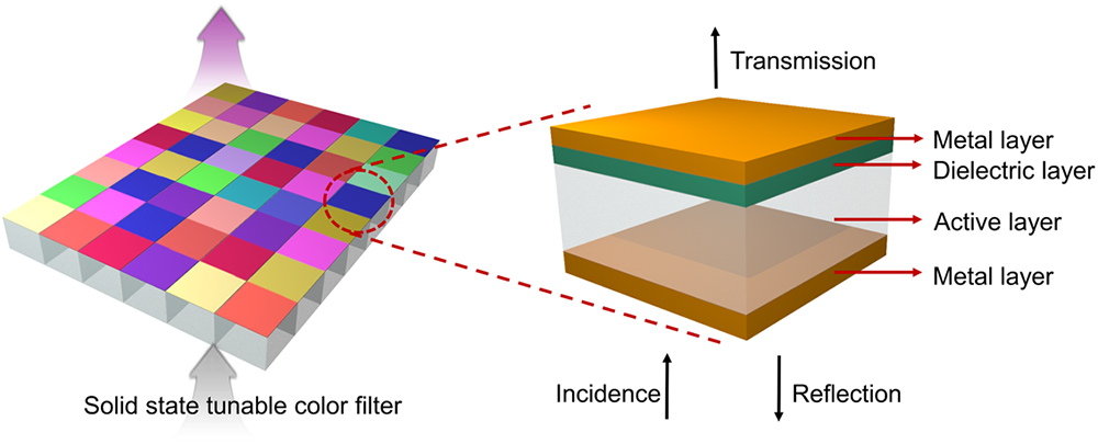
    Fig. 1. Schematic of the tunable all-solid-state color filter based on a doped semiconductor. The top and bottom metal layers are silver (Ag), the passive index-changing layer is IGZO, and the dielectric spacer layer is silicon dioxide (SiO2).
    Working mechanism of tunable color filter. (a) Schematic of tunable color filters. (b) The electron density and refractive index of the IGZO layer are changed under the H2 treatment process. The thickness of the semiconducting layer can be a few tens of nanometers. (c) Corresponding modulation of the refractive index and extinction coefficient depending on the electron density. The low conductivity film had an electron density of less than 1014 cm−3, and the high conductivity film had an electron density of 8×1019 cm−3. Both samples were made of identical materials, and only the electron density was controlled.
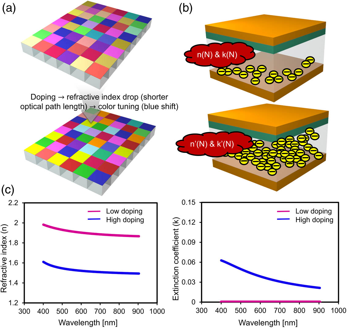
    Fig. 2. Working mechanism of tunable color filter. (a) Schematic of tunable color filters. (b) The electron density and refractive index of the IGZO layer are changed under the H2 treatment process. The thickness of the semiconducting layer can be a few tens of nanometers. (c) Corresponding modulation of the refractive index and extinction coefficient depending on the electron density. The low conductivity film had an electron density of less than 1014  cm3, and the high conductivity film had an electron density of 8×10¹⁹  cm3. Both samples were made of identical materials, and only the electron density was controlled.
    FDTD simulation results. (a) Simulation result of FP type transmission color filter. Top and bottom layers use Ag as a reflecting mirror. IGZO and SiO2 work as the dielectric spacing layer. IGZO is a transparent oxide layer and by a H2 treatment process, the charge concentration can be tuned. The transmitted colors are obtained by varying the thickness of the SiO2 layer. (The thickness increases from 40 nm to 180 nm in 20 nm steps.) (b) Color tuning before and after H2 treatment. (c), (d) Simulated transmission spectra are presented where the SiO2 layer thickness is (c) 60 nm and (d) 80 nm. (e), (f) Transmission spectrum plot as a function of wavelength and spacer thickness (e) before and (f) after H2 treatment.
    Fig. 3. FDTD simulation results. (a) Simulation result of FP type transmission color filter. Top and bottom layers use Ag as a reflecting mirror. IGZO and SiO2 work as the dielectric spacing layer. IGZO is a transparent oxide layer and by a H2 treatment process, the charge concentration can be tuned. The transmitted colors are obtained by varying the thickness of the SiO2 layer. (The thickness increases from 40 nm to 180 nm in 20 nm steps.) (b) Color tuning before and after H2 treatment. (c), (d) Simulated transmission spectra are presented where the SiO2 layer thickness is (c) 60 nm and (d) 80 nm. (e), (f) Transmission spectrum plot as a function of wavelength and spacer thickness (e) before and (f) after H2 treatment.
    Experimental results of centimeter-scale device. (a) Photograph of fabricated devices. The top row is the devices before H2 treatment, and the bottom row is the carrier-injected devices. The increase in carrier concentration can blue shift the wavelength peak of transmitted light resulting in color change from green to blue, for example. From left to right, the SiO2 layer increases from 40 nm to 120 nm. By increasing the thickness of the dielectric spacer, the wavelength is red shifted. The experimental results are well matched to the simulation results. Each sample size is 2 cm×2 cm. (b) Measured transmission spectrum from non-doped devices depending on the SiO2 layer thickness. (c) Color change map due to H2 treatment. The dielectric layer thickness of the sample moving from green to blue is 60 nm, and the purple to brown is 120 nm. The white triangle represents sRGB color space. (d) Measured transmission spectrum with SiO2 thickness of 120 nm.
    Fig. 4. Experimental results of centimeter-scale device. (a) Photograph of fabricated devices. The top row is the devices before H2 treatment, and the bottom row is the carrier-injected devices. The increase in carrier concentration can blue shift the wavelength peak of transmitted light resulting in color change from green to blue, for example. From left to right, the SiO2 layer increases from 40 nm to 120 nm. By increasing the thickness of the dielectric spacer, the wavelength is red shifted. The experimental results are well matched to the simulation results. Each sample size is 2  cm×2  cm. (b) Measured transmission spectrum from non-doped devices depending on the SiO2 layer thickness. (c) Color change map due to H2 treatment. The dielectric layer thickness of the sample moving from green to blue is 60 nm, and the purple to brown is 120 nm. The white triangle represents sRGB color space. (d) Measured transmission spectrum with SiO2 thickness of 120 nm.
    Experimental results of micro-sized color printing. The device consists of four layers including top and bottom layers of Ag surrounding IGZO and SiO2 layers. The color pixels were fabricated by an FIB process after the deposition of a 180 nm thick SiO2 layer. (a) Optical microscope images of 20 μm sized color pixels. (b) Colorful pictures with 1 μm sized color pixels. Left: low doping IGZO; right: high doping IGZO.
    Fig. 5. Experimental results of micro-sized color printing. The device consists of four layers including top and bottom layers of Ag surrounding IGZO and SiO2 layers. The color pixels were fabricated by an FIB process after the deposition of a 180 nm thick SiO2 layer. (a) Optical microscope images of 20 μm sized color pixels. (b) Colorful pictures with 1 μm sized color pixels. Left: low doping IGZO; right: high doping IGZO.
    Atomic force microscope (AFM) image. To characterize the fabricated micro-scale color pixel of a colorful picture, an AFM measurement was conducted. The 1 μm×1 μm sized pixel has different depths depending on the encoded color information. (a) Top view of AFM image. The depth is described as brightness value. (b) 3D AFM image. (c) Cross-section depth information of red-dashed line in (a). The y axis of the plot represents relative positions.
    Fig. 6. Atomic force microscope (AFM) image. To characterize the fabricated micro-scale color pixel of a colorful picture, an AFM measurement was conducted. The 1  μm×1  μm sized pixel has different depths depending on the encoded color information. (a) Top view of AFM image. The depth is described as brightness value. (b) 3D AFM image. (c) Cross-section depth information of red-dashed line in (a). The y axis of the plot represents relative positions.
    Refractive index modulation. Measured refractive index of IGZO film after different H2 plasma treatment conditions. Particularly, by changing the process temperature, the refractive index can be modulated. In this study, the H2 plasma treatment was performed at 120°C by a plasma-enhanced chemical vapor deposition chamber.
    Fig. 7. Refractive index modulation. Measured refractive index of IGZO film after different H2 plasma treatment conditions. Particularly, by changing the process temperature, the refractive index can be modulated. In this study, the H2 plasma treatment was performed at 120°C by a plasma-enhanced chemical vapor deposition chamber.
    Inki Kim, Juyoung Yun, Trevon Badloe, Hyuk Park, Taewon Seo, Younghwan Yang, Juhoon Kim, Yoonyoung Chung, Junsuk Rho. Structural color switching with a doped indium-gallium-zinc-oxide semiconductor[J]. Photonics Research, 2020, 8(9): 1409
    Download Citation