Abstract
Structural coloration techniques have improved display science due to their high durability in terms of resistance to bleaching and abrasion, and low energy consumption. Here, we propose and demonstrate an all-solid-state, large-area, lithography-free color filter that can switch structural color based on a doped semiconductor. Particularly, an indium-gallium-zinc-oxide (IGZO) thin film is used as a passive index-changing layer. The refractive index of the IGZO layer is tuned by controlling the charge carrier concentration; a hydrogen plasma treatment is used to control the conductivity of the IGZO layer. In this paper, we verify the color modulation using finite difference time domain simulations and experiments. The IGZO-based color filter technology proposed in this study will pave the way for charge-controlled tunable color filters displaying a wide gamut of colors on demand.1. INTRODUCTION
Structural coloration from metallic–dielectric nanostructures and subwavelength-sized thin films has been considered as an alternative to conventional color display technology [1–3]. Nanostructure-based coloration utilizes plasmonic [4,5] (in the case of metals) or multipolar electric and magnetic resonances (in the case of high index dielectrics [2]) in order to create high-resolution () [6] and vivid colors over a large gamut (comparable to Adobe RGB and approaching Rec2020) [7–9]. However, due to the lack of large-area nanopatterning techniques, practical applications of such nanostructure-based color are limited [10]. On the other hand, multilayer thin-film cavity-type structures, known as Fabry–Perot (FP) devices, do not require any expensive and time-consuming nanopatterning process. Therefore, they have an obvious advantage for making large-area devices that are also able to produce comparable vibrant colors [11–14]. However, both nanostructure- and thin-film-based coloration techniques have a common issue, which is “on demand” color switching.
There are three common methods for tuning nanostructure- and thin-film-based color filters: (1) mechanical deformation of the nanostructures; (2) polarization control; and (3) adopting phase change materials (PCMs), which have large differences in refractive indices in different phases [15]. A couple of examples of mechanical deformation methods are structural colors realized by nanoparticle arrays on flexible substrates that can be tuned by stretching or shirking to change the color [16], and using moisture (or liquid)-responsive materials, where the optical resonance can be tuned by swelling or deswelling the responsive layer [14,17,18]. The main problems of these approaches are the mechanical durability and limited experimental environment (such as a humidity-controlled chamber). The second approach is polarization control, which can be used for anisotropic nanostructures. Anisotropic structures (or adopting multiple nanostructures in a unit cell) can be used to tune the characteristics of scattered light by inducing different electromagnetic modes according to the polarization of the incident light [19–24]. The problem with this approach is that the tuning range is limited (e.g., simple rectangular nanobar shape) [21] to exhibit intensity modulation without significant color change. Also, in the case of using multiple nanostructures in a unit cell to broaden the tuning range [23], crosstalk between the scattered light from each structure can significantly reduce the efficiency of the device. The third approach, using PCMs, is being studied more actively. PCMs can also be divided into several categories depending on the type of external stimulus they react to: heat, chemical reaction, or external applied voltage. For example, [25,26] and [27–30] are widely known PCMs that change crystallinity due to joule heating. These materials are unsatisfactory for use in color filter applications, as their refractive index values change mostly in the near-infrared regime rather than the visible spectrum. Recently, a new PCM, , which has a wide bandgap and a significant index difference in the visible regime, has been reported [31]. These heat-reactive PCMs not only require high temperatures to undergo phase transitions ( changes phase at around 80°C, at 160°C, and higher than 200°C for ), but also the refractive index shift is not high enough to dramatically change the producible color. Chemically reactive PCMs, such as magnesium [32,33] and palladium [34], can be employed in dynamic color pixels, but most of them exhibit a coloration on/off function with a metal–insulator phase change, rather than color switching. Several electrically tunable PCMs such as liquid crystal [35], electrochromic materials [36,37], and indium tin oxide (ITO) [38] have been introduced, but their refractive index change at visible wavelengths is insufficient for use in structural color.
Recently, electrically tunable “solid-state” devices have been actively investigated. Solid-state devices are more advantageous than gas or liquid state devices because they quickly and reliably change the index of a material. Until now, a solid-state device was frequently implemented mainly by injecting ions in the solid layer. For instance, a lithium ion can be injected into a layer [39] or a hydrogen ion into a layer [40] to tune a refractive index. However, if the refractive index can be changed by a charge carrier or exciton [41] rather than by ion injection and ejection, it is expected that the optical properties of a tunable device can be changed more quickly and reliably with lower energy consumption.
Sign up for Photonics Research TOC. Get the latest issue of Photonics Research delivered right to you!Sign up now
Herein, as a proof of concept for a carrier-concentration-controlled tunable device, we propose an all-solid-state color filter that can switch structural color based on an indium-gallium-zinc-oxide (IGZO) passive index-changing layer in a metal–dielectric–IGZO–metal cavity structure. By controlling the carrier concentration in the IGZO layer, the refractive index in the visible regime can be controlled, and as a result, the color filter operates over the wide visible spectrum. This transmission-type color filter consists of four layers (Fig. 1), and the top and bottom metal layers work as mirrors in the FP resonator.
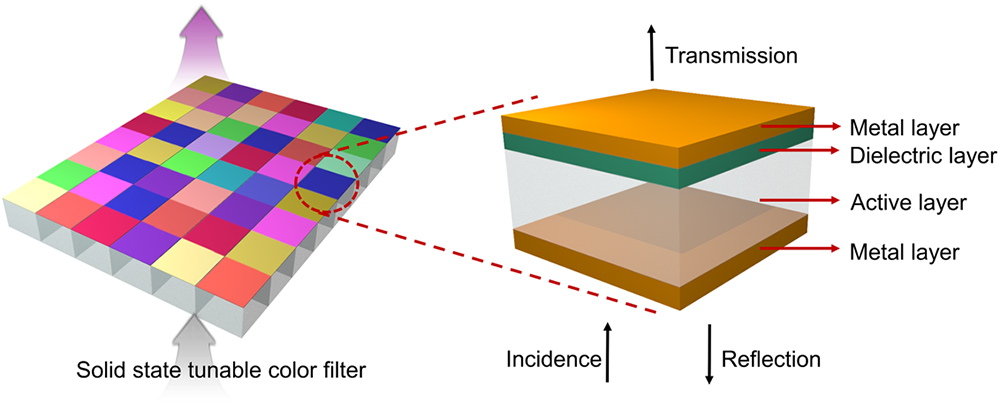
Figure 1.Schematic of the tunable all-solid-state color filter based on a doped semiconductor. The top and bottom metal layers are silver (Ag), the passive index-changing layer is IGZO, and the dielectric spacer layer is silicon dioxide ().
2. RESULTS AND DICUSSION
IGZO is a promising semiconductor material used widely in thin-film transistors for flat panel display [42]. This oxide material exhibits superior electric/optical properties such as high carrier mobility, high transparency, and large-area uniformity. Applications of IGZO include high-resolution display [43], sensors [44,45], and thin-film circuits [46]. Despite these advantages, IGZO has yet to be used in photonic device applications.
In solids, the electric polarization is modeled as permittivity, which is affected by microscopic interactions between electric fields and charged elements. This microscopic phenomenon is related to the macroscopic parameters, refractive index, and extinction coefficient, which represent how light propagates in a medium. Our main idea is to control the carrier concentration in an optically transparent solid thin film. If the density or conductivity is sufficiently modulated, the electric polarization and plasma frequency are changed, which in turn modulates the optical properties of the thin film. Because the refractive index is controlled in a transparent medium, the effects of modulation are valid in the wide visible spectrum (Fig. 2).

Figure 2.Working mechanism of tunable color filter. (a) Schematic of tunable color filters. (b) The electron density and refractive index of the IGZO layer are changed under the treatment process. The thickness of the semiconducting layer can be a few tens of nanometers. (c) Corresponding modulation of the refractive index and extinction coefficient depending on the electron density. The low conductivity film had an electron density of less than , and the high conductivity film had an electron density of . Both samples were made of identical materials, and only the electron density was controlled.
The electron density of IGZO is an essential factor to modulate the refractive index. A 40 nm thick transparent semiconductor thin film of IGZO was deposited, and its electron density was controlled with a plasma treatment process. Free electrons are generated with plasma because the injected hydrogen atom forms O-H bonds with ionized oxygens in IGZO as the following reaction [47]:
The modulation of the IGZO refractive index can be explained by the Tauc–Lorentz–Drude (TL-Drude) model. The TL-Drude model was previously used to model optical properties of oxide semiconductors such as ZnO and [46]. The dielectric constant of the TL-Drude model is expressed as where and represent the dielectric constants given by the TL and Drude models, respectively. The dielectric constant of the TL term describes the band-to-band energy absorption, and the Drude term describes free-electron absorption. Although the Drude model is commonly used to analyze metallic materials, it can be applied to doped IGZO, as plasma treatment increases the electron density similar to metallic materials. The complex dielectric constant of the Drude model is expressed as [48,49] where and are real and imaginary parts of , respectively. and represent the amplitude and broadening parameters, respectively. is expressed as where is plasma energy, is the Planck constant, is plasma angular frequency, is carrier concentration, is electron charge, and is free-space permittivity.
The refractive index of IGZO can be obtained from the relationship between the dielectric constant and refractive index: where are the real and imaginary parts of complex dielectric constant, respectively. Based on Eq. (6), the refractive index decreases because decreases while increases as a result of the increasing electron density.
Ar bombardment during plasma treatment, however, cannot be neglected, as it can break the oxygen bond and generate oxygen vacancies [50]. Oxygen vacancies act as deep-level traps so that a highly doped IGZO film absorbs light with energy lower than its bandgap. Figure 2(c) describes an increase in extinction coefficient at lower energy than the bandgap. Furthermore, the Ar bombardment can reduce the refractive index by increasing the electron density of the IGZO film due to oxygen vacancy.
The low conductive IGZO sample had an electron density of less than , and the highly conductive film had an electron density of . Ellipsometry measurements were performed to extract the optical properties. As shown in Fig. 2, the refractive index varied by over the entire visible spectrum, and the extinction coefficient also varied as the film conductance changed. This result provides the basis for refractive index modulation in a solid thin film by varying the electron density. However, the electron density needs to be further controlled by voltage to realize an electrically controlled active-index thin film.
The color filter takes the shape of an FP resonator. The resonance conditions of an FP resonator are determined by the constructive and destructive interference caused by specific phase shift at the metal interfaces as the light reflects within the resonator. For this reason, not only a very sharp resonance peak can be obtained in the FP resonator, but also a high transmittance can be obtained since the FP resonator does not rely on the use of plasmons. The device consists of four layers, top and bottom silver (Ag) layers with silicon dioxide () and IGZO layers in between. It is confirmed by finite difference time domain (FDTD) simulations that the color is tuned when the thickness and carrier concentration are changed [Fig. 3(a)]. The refractive index of the IGZO layer was modeled by the measured ellipsometry results [Fig. 2(c)]. As the thickness of increases, the resonance wavelength is red shifted as the optical path length becomes longer. More importantly, increasing carrier concentration of the IGZO layer lowers the refractive index in the IGZO layer, which means that the optical path length decreases, so blue shifting of the resonance peak, i.e., tuning color, is possible. Figure 3(b) describes the color tuning on the CIE 1931 color space chromaticity diagram before and after the treatment, and the corresponding calculated spectra are shown in Fig. 3(c), where the resonance wavelength shift is around 60 nm. Figure 3(d) shows the result when the layer is 80 nm thick. Furthermore, as shown in Figs. 3(e) and 3(f), the transmission plot as a function of wavelength and spacer thickness shows the tendency that the resonance wavelength shift before and after treatment becomes smaller as the thickness increases. Considering the very thin accumulation layer thickness of the IGZO layer compared to entire dielectric spacing layer (), the thicker the spacing layer becomes, the smaller the wavelength shift is.
Figure 3.FDTD simulation results. (a) Simulation result of FP type transmission color filter. Top and bottom layers use Ag as a reflecting mirror. IGZO and work as the dielectric spacing layer. IGZO is a transparent oxide layer and by a treatment process, the charge concentration can be tuned. The transmitted colors are obtained by varying the thickness of the layer. (The thickness increases from 40 nm to 180 nm in 20 nm steps.) (b) Color tuning before and after treatment. (c), (d) Simulated transmission spectra are presented where the layer thickness is (c) 60 nm and (d) 80 nm. (e), (f) Transmission spectrum plot as a function of wavelength and spacer thickness (e) before and (f) after treatment.
The color filter devices were fabricated by using an electron beam evaporation method (for 30 nm thick Ag and layers) and a sputtering method (for a 40 nm thick IGZO layer) at high vacuum followed by a treatment process [Fig. 4(a)]. Five devices were made with increasing thicknesses from 40 nm to 120 nm in 20 nm steps, and the transmitted colors were observed. Consistent with the simulation results, increasing the dielectric layer thickness resulted in a red shift of the resonance wavelength, which was confirmed by spectral measurement. The five samples in the top row of Fig. 4(a) are before the treatment, and in the bottom row are after the treatment with layers, which increase in thickness from 40 nm to 120 nm (left to right). After the treatment, the thickness of the IGZO layer was found to have a negligible change, and thus the color change of the sample was due purely to the change in the refractive index of the IGZO layer. Again, consistent with the simulation results, the resonance wavelength blue shifts as the refractive index decreases with the treatment. As shown on the CIE 1931 chromaticity diagram [Figs. 4(c) and 4(d)], the color difference between the before and after treatment states is significant, due to the change of refractive index []. The decreased transmission of the measured transmission compared to the simulated results is expected to be due to the surface quality of the IGZO layer, which was affected by the treatment and following Ar bombardment processes. In addition to this kind of large-area color filter, micro-sized color printing is also possible using electron beam lithography or a focused ion beam (FIB) milling method (Fig. 5). Using an FIB process, 20 μm sized color pixels were fabricated. According to the depth variation controlled by milling time, various vivid colors can be produced. Furthermore, colorful pictures with a 1 μm sized pixel are also experimentally demonstrated. Each pixel of the fabricated device has several tens of nanometers scale depth and is very difficult to measure using a scanning electron microscope, so the device is characterized using an atomic force microscope (Fig. 6).
Figure 4.Experimental results of centimeter-scale device. (a) Photograph of fabricated devices. The top row is the devices before treatment, and the bottom row is the carrier-injected devices. The increase in carrier concentration can blue shift the wavelength peak of transmitted light resulting in color change from green to blue, for example. From left to right, the layer increases from 40 nm to 120 nm. By increasing the thickness of the dielectric spacer, the wavelength is red shifted. The experimental results are well matched to the simulation results. Each sample size is . (b) Measured transmission spectrum from non-doped devices depending on the layer thickness. (c) Color change map due to treatment. The dielectric layer thickness of the sample moving from green to blue is 60 nm, and the purple to brown is 120 nm. The white triangle represents sRGB color space. (d) Measured transmission spectrum with thickness of 120 nm.
Figure 5.Experimental results of micro-sized color printing. The device consists of four layers including top and bottom layers of Ag surrounding IGZO and layers. The color pixels were fabricated by an FIB process after the deposition of a 180 nm thick layer. (a) Optical microscope images of 20 μm sized color pixels. (b) Colorful pictures with 1 μm sized color pixels. Left: low doping IGZO; right: high doping IGZO.
Figure 6.Atomic force microscope (AFM) image. To characterize the fabricated micro-scale color pixel of a colorful picture, an AFM measurement was conducted. The sized pixel has different depths depending on the encoded color information. (a) Top view of AFM image. The depth is described as brightness value. (b) 3D AFM image. (c) Cross-section depth information of red-dashed line in (a). The axis of the plot represents relative positions.
3. CONCLUSION
We have proposed an all-solid-state color filter that can switch structural colors based on the doping level of IGZO, a material used widely in thin-film transistors for flat panel displays. The treatment changes the charge concentration of the IGZO layer from to , resulting in a refractive index difference of 0.4 over the entire visible region maintaining a negligible extinction coefficient. We fabricated an FP-type resonator structure containing an IGZO layer and verified dramatic color changes in the visible region through FDTD simulations and experiments. Although the device presented here is in transmission mode, it can easily be used in reflection mode to produce a subtractive color palette. IGZO has many advantages in terms of promising use for electrically tunable photonics devices such as good uniformity over a large area, sufficient thickness for a charge accumulation layer, and significant index modulation in the visible regime. Furthermore, once the charge concentration of the IGZO layer can be controlled by an electrical bias, IGZO-based devices are expected to be an important platform for electrically tunable optical devices working at visible wavelengths. Also, machine learning technology, which has been actively studied in recent years, can be applied to highly efficient color filter design that can realize more vivid colors [51,52].
4. METHODS
A. Device Fabrication
The IGZO tunable color filters were fabricated on a fused silica substrate. First, a 30 nm thick Ag thin film and different thicknesses of silica layers were deposited by electron beam evaporation with rates of and , respectively. Then, an IGZO layer (40 nm) was deposited by an RF sputtering system at room temperature. The composition of the IGZO target was 1:1:1 (mole ratio) of In:Ga:Zn. The sputtering was performed under Ar atmosphere. After the sputtering, the film was annealed at 300°C for 2 h under atmosphere. plasma treatment was then performed at 120°C by a plasma-enhanced chemical vapor deposition chamber for 5 min with RF power of 200 W. Also, depending on the plasma treatment, the refractive index could be modulated (Fig. 7). FIB milling was used to produce the micro-sized color pixel and corresponding color picture (FEI, Helios NanoLab DualBeam). Particularly, in order to fabricate differently colored pixels, the milling depth should be different for each pixel. So we prepared five CAD files arranged in a rectangular array with a spacing of 200 nm and a size of to produce five different colors. For the FIB process, first a 180 nm thick layer was deposited, and by varying the ion milling time, the final layer thickness was adjusted. After the milling process, the IGZO and Ag layers were coated.
Figure 7.Refractive index modulation. Measured refractive index of IGZO film after different plasma treatment conditions. Particularly, by changing the process temperature, the refractive index can be modulated. In this study, the plasma treatment was performed at 120°C by a plasma-enhanced chemical vapor deposition chamber.
B. Optical Characterization
The optical measurements (transmittance) were performed using Fourier transform infrared spectroscopy (Bruker, Vertex 70) with a microscope (Bruker, Hyperion 2000) in transmission mode.
C. Simulations
All simulations were done using the commercially available FDTD package Lumerical Solutions. 2D simulation regions were set up with periodic boundary conditions in the direction and perfectly matched layers at the boundaries. A plane wave was injected in the backward direction, and the transmission was calculated 200 nm below the bottom Ag layer. The values for the refractive index of and Ag were taken from the material library, while the refractive index of IGZO was modeled using the data measured using ellipsometry for films of high- and low-doping samples.
Acknowledgment
Acknowledgment. I.K. acknowledges the Global Ph.D. fellowship (NRF-2016H1A2A1906519) and Y.Y. acknowledges the Hyundai Motor Chung Mong-Koo Foundation fellowship.
References
[1] A. Kristensen, J. K. W. Yang, S. I. Bozhevolnyi, S. Link, P. Nordlander, N. J. Halas, N. A. Mortensen. Plasmonic colour generation. Nat. Rev. Mater., 2, 16088(2016).
[2] T. Lee, J. Jang, H. Jeong, J. Rho. Plasmonic- and dielectric-based structural coloring: from fundamentals to practical applications. Nano Converg., 5, 1(2018).
[3] I. Kim, G. Yoon, J. Jang, P. Genevet, K. T. Nam, J. Rho. Outfitting next generation displays with optical metasurfaces. ACS Photon., 5, 3876-3895(2018).
[4] C. U. Hail, G. Schnoering, M. Damak, D. Poulikakos, H. Eghlidi. A plasmonic painter’s method of color mixing for a continuous red-green-blue palette. ACS Nano, 14, 1783-1791(2020).
[5] M. Song, D. Wang, S. Peana, S. Choudhury, P. Nyga, Z. A. Kudyshev, H. Yu, A. Boltasseva, V. M. Shalaev, A. V. Kildishev. Colors with plasmonic nanostructures: a full-spectrum review. Appl. Phys. Rev., 6, 041308(2019).
[6] K. Kumar, H. Duan, R. S. Hegde, C. W. Koh, J. N. Wei, J. K. W. Yang. Printing color at the optical diffraction limit. Nat. Nanotechnol., 7, 557-561(2012).
[7] B. Yang, W. Liu, Z. Li, H. Cheng, D.-Y. Choi, S. Chen, J. Tian. Ultrahighly saturated structural colors enhanced by multipolar-modulated metasurfaces. Nano Lett., 19, 4221-4228(2019).
[8] J.-H. Yang, V. E. Babicheva, M.-W. Yu, T.-C. Lu, T.-R. Lin, K.-P. Chen. Structural colors enabled by lattice resonance on silicon nitride metasurfaces. ACS Nano, 14, 5678-5685(2020).
[9] W. Yang, S. Xiao, Q. Song, Y. Liu, Y. Wu, S. Wang, J. Yu, J. Han, D.-P. Tsai. All-dielectric metasurface for high-performance structural color. Nat. Commun., 11, 1864(2020).
[10] E. Højlund-Nielsen, J. Clausen, T. Mäkela, L. H. Thamdrup, M. Zalkovskij, T. Nielsen, N. L. Pira, J. Ahopelto, N. A. Mortensen, A. Kristensen. Plasmonic colors: toward mass production of metasurfaces. Adv. Mater. Technol., 1, 1600054(2016).
[11] Z. Li, S. Butun, K. Aydin. Large-area, lithography-free super absorbers and color filters at visible frequencies using ultrathin metallic films. ACS Photon., 2, 183-188(2015).
[12] S.-J. Kim, H.-K. Choi, H. Lee, S.-H. Hong. Solution-processable nanocrystal-based broadband Fabry–Perot absorber for reflective vivid color generation. ACS Appl. Mater. Interface, 11, 7280-7287(2019).
[13] C. Williams, G. S. D. Gordon, T. D. Wilkinson, S. E. Bohndiek. Grayscale-to-color: scalable fabrication of custom multispectral filter arrays. ACS Photon., 6, 3132-3141(2019).
[14] J. Jang, K. Kang, N. Raeis-Hosseini, A. Ismukhanova, H. Jeong, C. Jeong, B. Kim, J.-Y. Lee, I. Park, J. Rho. Self-powered humidity sensor using chitosan-based plasmonic metal-hydrogel-metal filters. Adv. Opt. Mater., 8, 1901932(2020).
[15] S. Bang, J. Kim, G. Yoon, T. Tanaka, J. Rho. Recent advances in tunable and reconfigurable metamaterials. Micromachines, 9, 560(2018).
[16] M. L. Tseng, J. Yang, M. Semmlinger, C. Zhang, P. Nordlander, N. J. Halas. Two-dimensional active tuning of an aluminum plasmonic array for full-spectrum response. Nano Lett., 17, 6034-6039(2017).
[17] H. Kwon, S. Kim. Chemically tunable, biocompatible, and cost-effective metal-insulator-metal resonators using silk protein and ultrathin silver films. ACS Photon., 2, 1675-1680(2015).
[18] S. D. Rezaei, J. Ho, A. Naderi, M. T. Yaraki, T. Wang, Z. Dong, S. Ramakrishna, J. K. W. Yang. Tunable, cost-effective, and scalable structural colors for sensing and consumer products. Adv. Opt. Mater., 7, 1900735(2019).
[19] Y. Nagasaki, M. Suzuki, J. Takahara. All-dielectric dual-color pixel with subwavelength resolution. Nano Lett., 17, 7500-7506(2017).
[20] B. Yang, W. Liu, Z. Li, H. Cheng, S. Chen, J. Tian. Polarization-sensitive structural colors with hue-and-saturation tuning based on all-dielectric nanopixels. Adv. Opt. Mater., 6, 1701009(2018).
[21] J. Jang, H. Jeong, G. Hu, C.-W. Qiu, K. T. Nam, J. Rho. Tunable metasurfaces: Kerker-conditioned dynamics cryptographic nanoprints. Adv. Opt. Mater., 7, 1970016(2019).
[22] M. Kim, I. Kim, J. Jang, D. Lee, K. T. Nam, J. Rho. Active color control in a metasurface by polarization rotation. Appl. Sci., 8, 982(2018).
[23] H. Yun, S.-Y. Lee, K. Hong, J. Yeom, B. Lee. Plasmonic cavity-apertures as dynamic pixels for the simultaneous control of colour and intensity. Nat. Commun., 6, 7133(2015).
[24] H.-E. Lee, H.-Y. Ahn, J. Mun, Y. Y. Lee, M. Kim, N. H. Cho, K. Chang, W. S. Kim, J. Rho, K. T. Nam. Amino-acid- and peptide-directed synthesis of chiral plasmonic gold nanoparticles. Nature, 556, 360-365(2018).
[25] F.-Z. Shu, F.-F. Yu, R.-W. Peng, Y.-Y. Zhu, B. Xiong, R.-H. Fan, Z.-H. Wang, Y. Liu, M. Wang. Dynamic plamonic color generation based on phase transition of vanadium dioxide. Adv. Opt. Mater., 6, 1700939(2018).
[26] T. Badloe, I. Kim, J. Rho. Moth-eye shaped on-demand broadband and switchable perfect absorbers based on vanadium dioxide. Sci. Rep., 10, 4522(2020).
[27] P. Hosseini, C. D. Wright, H. Bhaskaran. An optoelectronic framework enabled by low-dimensional phase-change films. Nature, 511, 206-211(2014).
[28] S. Yoo, T. Gwon, T. Eom, S. Kim, C. S. Hwang. Multicolor changeable optical coating by adopting multiple layers of ultrathin phase change material film. ACS Photon., 3, 1265-1270(2016).
[29] N. Raeis-Hosseini, S. Lim, H. Hwang, J. Rho. Reliable Ge2Sb2Te5-integrated high-density nanoscale conductive bridge random access memory using facile nitrogen-doping strategy. Adv. Electron. Mater., 4, 1800360(2018).
[30] N. Raeis-Hosseini, J. Rho. Dual-functional nanoscale devices using phase change materials: reconfigurable perfect absorber with nonvolatile resistance-change memory characteristics. Appl. Sci., 9, 564(2019).
[31] W. Dong, H. Liu, J. K. Behera, L. Lu, R. J. H. Ng, K. V. Sreekanth, X. Zhou, J. K. W. Yang. Wide bandgap change material tuned visible photonics. Adv. Funct. Mater., 29, 1806181(2019).
[32] X. Y. Duan, S. Kamin, N. Liu. Dynamic plasmonic colour display. Nat. Commun., 8, 14606(2017).
[33] Y. Chen, X. Y. Duan, M. Matuschek, Y. Zhou, F. Neubrech, H. G. Duan, N. Liu. Dynamic color displays using stepwise cavity resonators. Nano Lett., 17, 5555-5560(2017).
[34] N. Liu, M. L. Tang, M. Hentschel, H. Giessen. Nanoantenna-enhanced gas sensing in a single tailored nanofocus. Nat. Mater., 10, 631-636(2011).
[35] D. Franklin, Y. Chen, A. Vazquez-Guardado, S. Modak, J. Boroumand, D. Xu, S.-T. Wu, D. Chanda. Polarization-independent actively tunable colour generation on imprinted plasmonic surfaces. Nat. Commun., 6, 7337(2015).
[36] K. Xiong, D. Tordera, G. Emilsson, O. Olsson, U. Linderhed, M. P. Jonsson, A. B. Dahlin. Switchable plasmonic metasurfaces with high chromaticity containing only abundant metals. Nano Lett., 17, 7033-7039(2017).
[37] J. Peng, H.-H. Jeong, Q. Lin, S. Cormier, H.-L. Liang, M. F. L. De Volder, S. Vignolini, J. J. Baumberg. Scalable electrochromic nanopixels using plasmonics. Sci. Adv., 5, eaaw2205(2019).
[38] G. Yoon, S. So, M. Kim, J. Mun, R.-M. Ma, J. Rho. Electrically tunable metasurface perfect absorber for infrared frequencies. Nano Converg., 4, 36(2017).
[39] Y. Li, J. van de Groep, A. A. Talin, M. L. Brongersma. Dynamic tuning of gap plasmon resonances using a solid-state electrochromic device. Nano Lett., 19, 7988-7995(2019).
[40] M. Huang, A. J. Tan, F. Büttner, H. Liu, Q. Ruan, W. Hu, C. Mazzoli, S. Wilkins, C. Duan, J. K. W. Yang, G. S. D. Beach. Voltage-gated optics and plasmonics enabled by solid-state proton pumping. Nat. Commun., 10, 5030(2019).
[41] Y. Yu, Y. Yu, L. Huang, H. Peng, L. Xiong, L. Cao. Giant gating tunability of optical refractive index in transition metal dichalcogenide monolayers. Nano Lett., 17, 3613-3618(2017).
[42] H. Hosono. How we made the IGZO transistor. Nat. Electron., 1, 428(2018).
[43] J. K. Jeong, J. H. Jeong, J. H. Choi, J. S. Im, S. H. Kim, H. W. Yang, K. N. Kang, K. S. Kim, T. K. Ahn, H.-J. Chung, M. Kim, B. S. Gu, J.-S. Park, Y.-G. Mo, H. D. Kim. 3.1: Distinguished Paper: 12.1-inch WXGA AMOLED display driven by indium-gallium-zinc oxide TFTs array. SID Symp. Dig. Tech. Pap., 39, 1-4(2008).
[44] D. Geng, S. Han, H. Seo, M. Mativenga, J. Jang. Piezoelectric pressure sensing device using top-gate effect of dual-gate a-IGZO TFT. IEEE Sens. J., 17, 585-586(2017).
[45] Y.-H. Tai, H.-L. Chiu, L.-S. Chou. Active matrix touch sensor detecting time-constant change implemented by dual-gate IGZO TFTs. Solid-State Electron., 72, 67-72(2012).
[46] H. Chen, Y. Cao, J. Zhang, C. Zhou. Large-scale complementary macroelectronics using hybrid integration of carbon nanotubes and IGZO thin-film transistors. Nat. Commun., 5, 4097(2014).
[47] T. Kamiya, K. Nomura, H. Hosono. Present status of amorphous In-Ga-Zn-O thin-film transistors. Sci. Tech. Adv. Mater., 11, 044305(2010).
[48] H. Fujiwara, M. Kondo. Effects of carrier concentration on the dielectric function of ZnO:Ga and In2O3:Sn studied by spectroscopic ellipsometry: analysis of free-carrier and band-edge absorption. Phys. Rev. B, 71, 075109(2005).
[49] X. D. Li, S. Chen, T. P. Chen, Y. Liu. Thickness dependence of optical properties of amorphous indium gallium zinc oxide thin films: effects of free-electrons and quantum confinement. ECS Solid State Lett., 4, P29-P32(2015).
[50] J.-S. Park, J. K. Jeong, Y.-G. Mo, H. D. Kim, S.-I. Kim. Improvements in the device characteristics of amorphous indium gallium zinc oxide thin-film transistors by Ar plasma treatment. Appl. Phys. Lett., 90, 262106(2007).
[51] I. Sajedian, T. Badloe, J. Rho. Optimization of colour generation from dielectric nanostructures using reinforcement learning. Opt. Express, 27, 5874-5883(2019).
[52] T. Badloe, I. Kim, J. Rho. Biomimetic ultra-broadband perfect absorbers optimized with reinforcement learning. Phys. Chem. Chem. Phys., 22, 2337-2342(2020).


