• Journal of Semiconductors
  • Vol. 42, Issue 6, 062801 (2021)
Kyuhyun Cha1 and Kwangsoo Kim2
Author Affiliations
  • 1Department of Electronic Engineering, Sogang University, Seoul 04107, Korea
  • 2Department of Electronic Engineering, Sogang University, Seoul 04107, Korea
  • show less
    DOI: 10.1088/1674-4926/42/6/062801 Cite this Article
    Kyuhyun Cha, Kwangsoo Kim. 3.3 kV 4H-SiC DMOSFET with a source-contacted dummy gate for high-frequency applications[J]. Journal of Semiconductors, 2021, 42(6): 062801 Copy Citation Text show less
    (Color online) Schematic cross-sectional structure of (a) C-MOSFET, (b) CI-MOSFET, and (c) DG-MOSFET.
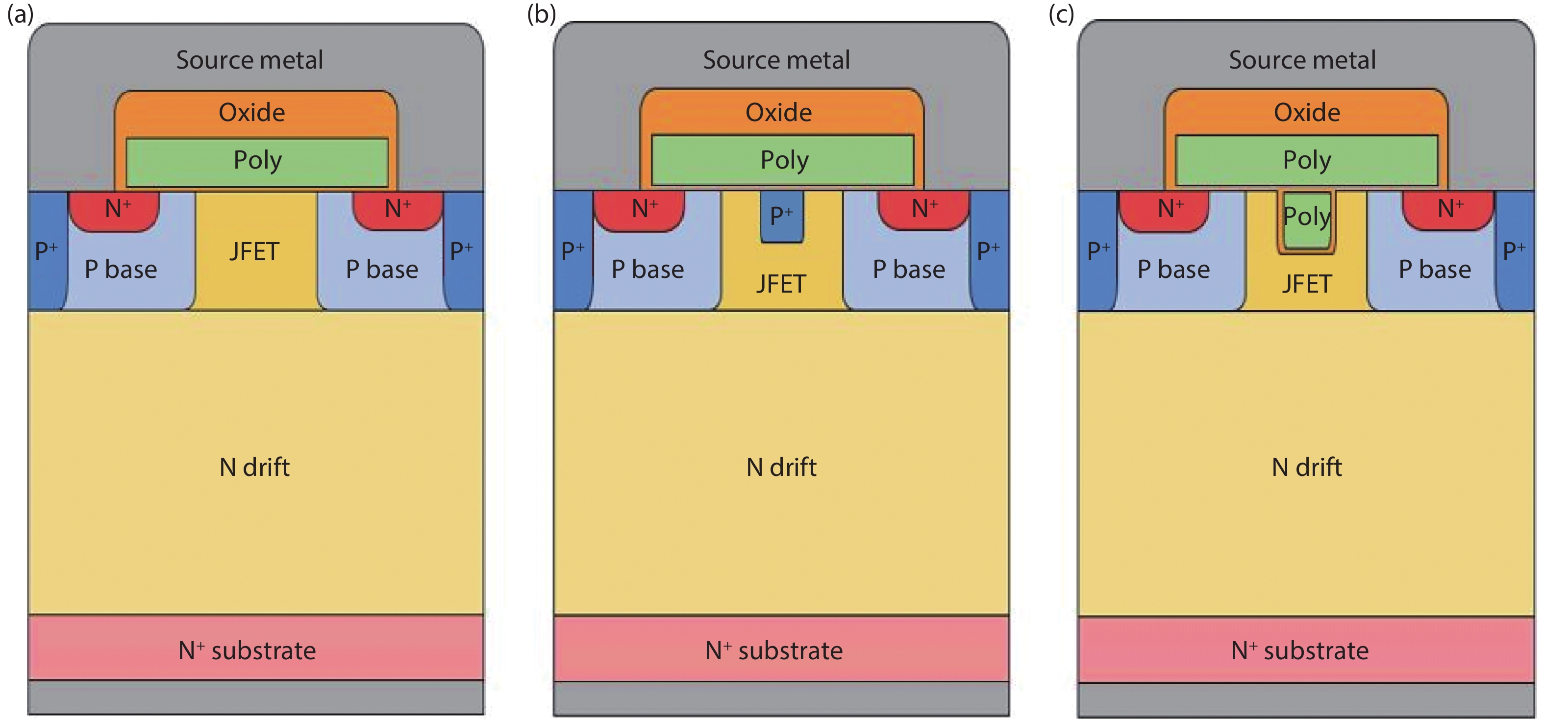
    Fig. 1. (Color online) Schematic cross-sectional structure of (a) C-MOSFET, (b) CI-MOSFET, and (c) DG-MOSFET.
    (Color online) Proposed key fabrication process flow of DG-MOSFET. (a) Ion implantation to form the p-well and n+ source. (b) Dummy etching. (c) Dummy oxide deposition. (d) Nitride mask removal & poly-Si deposition. (e) Poly-Si etchback. (f) Gate oxidation and patterning.
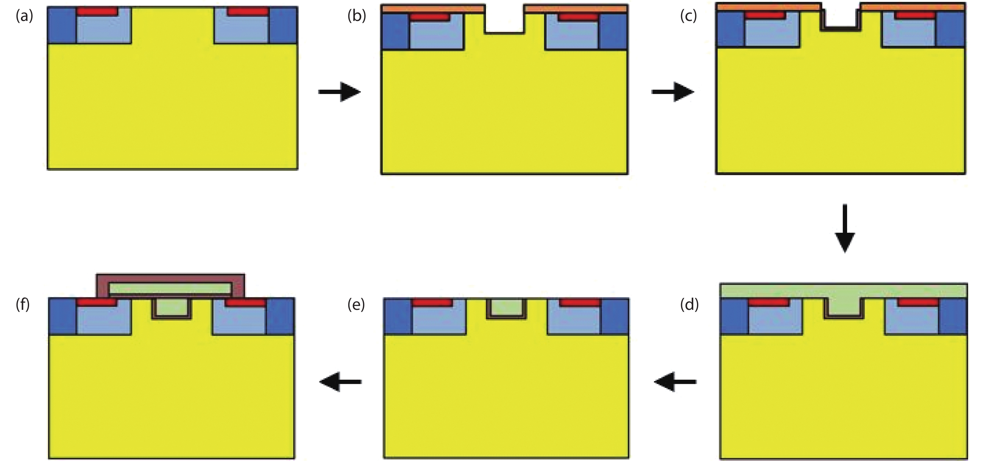
    Fig. 2. (Color online) Proposed key fabrication process flow of DG-MOSFET. (a) Ion implantation to form the p-well and n+ source. (b) Dummy etching. (c) Dummy oxide deposition. (d) Nitride mask removal & poly-Si deposition. (e) Poly-Si etchback. (f) Gate oxidation and patterning.
    (Color online) Influences of WJF and NJF of C-MOSFET. (a) The trade-off between RON and BV and (b) RON and EMOX (EMOX was measured at VDS = 3300 V.).
    Fig. 3. (Color online) Influences of WJF and NJF of C-MOSFET. (a) The trade-off between RON and BV and (b) RON and EMOX (EMOX was measured at VDS = 3300 V.).
    (Color online) Changes of FOM according to WJF and NJF of C-MOSFET.
    Fig. 4. (Color online) Changes of FOM according to WJF and NJF of C-MOSFET.
    (Color online) The trade-off between RON and BV as variation of WCI and DCI.
    Fig. 5. (Color online) The trade-off between RON and BV as variation of WCI and DCI.
    (Color online) FOM as a variation of WCI and DCI.
    Fig. 6. (Color online) FOM as a variation of WCI and DCI.
    (Color online) Influences of WDG and DDG of DG-MOSFET. (a) Trade-off between RON and BV and (b) RON and EMOX (EMOX was measured at VDS = 3300 V.).
    Fig. 7. (Color online) Influences of WDG and DDG of DG-MOSFET. (a) Trade-off between RON and BV and (b) RON and EMOX (EMOX was measured at VDS = 3300 V.).
    (Color online) Electric field distribution of three structures at VDS = 3300 V. (a) C-MOSFET. (b) CI-MOSFET. (c) DG-MOSFET.
    Fig. 8. (Color online) Electric field distribution of three structures at VDS = 3300 V. (a) C-MOSFET. (b) CI-MOSFET. (c) DG-MOSFET.
    (Color online) Static characteristics of three structures.
    Fig. 9. (Color online) Static characteristics of three structures.
    (Color online) Input and Gate-Drain capacitance of three structures.
    Fig. 10. (Color online) Input and Gate-Drain capacitance of three structures.
    (Color online) Gate-drain charge curve of three structures.
    Fig. 11. (Color online) Gate-drain charge curve of three structures.
    (Color online) (a) Turn off and (b) turn on transient of the three structures.
    Fig. 12. (Color online) (a) Turn off and (b) turn on transient of the three structures.
    (a) Buck converter and (b) boost converter circuit used in the power loss simulation.
    Fig. 13. (a) Buck converter and (b) boost converter circuit used in the power loss simulation.
    (Color online) Switching power loss in the power circuit. (a) Buck converter. (b) Boost converter.
    Fig. 14. (Color online) Switching power loss in the power circuit. (a) Buck converter. (b) Boost converter.
    ParameterC-MOSFETCI-MOSFETDG-MOSFET
    RON (mΩ∙cm2) 10.3412.0111.91
    BV (V)330533743343
    FOM (MW/cm2) 1056947934
    Table 1. Static characteristics of the optimized three structures.
    ParameterC-MOSFETCI-MOSFETDG-MOSFET
    CRSS and CGD were simulated at VDS = 1000 V and QGD was simulated at IGS = 100 mA and VDD = 1700 V.
    CISS (nF/cm2) 14.821.925.7
    CGD (pF/cm2) 66.6721.1219.36
    QGD (nC/cm2) 353.1159.5125.3
    RON×QGD (mΩ∙nC) 365119161492
    Table 2. Capacitance and gate charge values of the three structures.
    ParameterC-MOSFETCI-MOSFETDG-MOSFET
    EON (mJ/cm2) 41.917.2716.03
    EOFF (mJ/cm2) 11.277.847.68
    ESW (mJ/cm2) 53.1725.1123.71
    Table 3. Double-pulse test simulation results.
    Power circuitC-MOSFETCI-MOSFETDG-MOSFET
    Buck converter (kW)20.6168.9347.784
    Boost converter (kW)48.73120.92318.901
    Table 4. Power simulation results (f = 500 kHz).
    Kyuhyun Cha, Kwangsoo Kim. 3.3 kV 4H-SiC DMOSFET with a source-contacted dummy gate for high-frequency applications[J]. Journal of Semiconductors, 2021, 42(6): 062801
    Download Citation