
Kyuhyun Cha, Kwangsoo Kim. 3.3 kV 4H-SiC DMOSFET with a source-contacted dummy gate for high-frequency applications[J]. Journal of Semiconductors, 2021, 42(6): 062801
- Journal of Semiconductors
- Vol. 42, Issue 6, 062801 (2021)
Abstract
1. Introduction
4H-SiC is a wide bandgap material with excellent material properties, such as high critical electric field, high thermal conductivity, and high-temperature operation, making it suitable for high-temperature and high-voltage environments[
Among SiC MOSFET structures, the trench MOSFET has a low channel resistance thanks to its high channel density and mobility[
In previous studies, a central-implant MOSFET (CI-MOSFET) with a p+ region under the gate oxide was proposed to improve the switching characteristics of the conventional DMOSFET (C-MOSFET)[
Therefore, we propose a 3.3 kV dummy-gate 4H-SiC MOSFET (DG-MOSFET) to alleviate this problem. The static characteristics of the DG-MOSFET were analyzed through a Sentaurus TCAD 2D simulation, and the dynamic characteristics were analyzed through a mixed-mode simulation[
2. Proposed structure and fabrication procedure
2.1. Structures of DG-MOSFETs
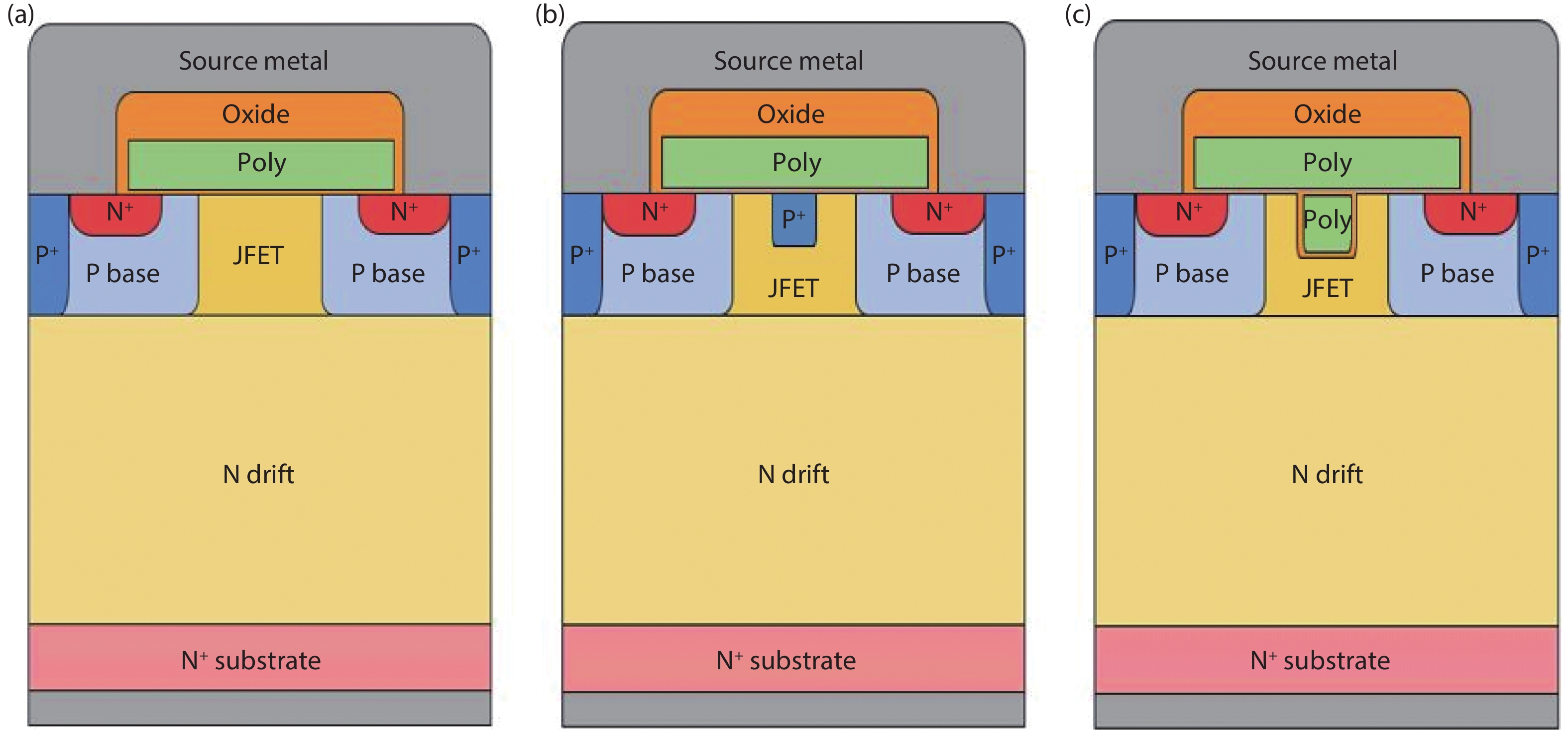
Fig. 1 shows the cross-sectional schematics of the C-MOSFET, CI-MOSFET, and DG-MOSFET. All of the structures have the same drift thickness (i.e., 30 μm) and the concentration of the drift region is 1.7 × 1015 cm−3. The junction depth of the p base is 1 μm. In the DG-MOSFET, CGD was reduced using the source-contacted DG structure under an active gate to reduce the overlapping region between the gate and the drain[
![]()
Figure 1.(Color online) Schematic cross-sectional structure of (a) C-MOSFET, (b) CI-MOSFET, and (c) DG-MOSFET.
2.2. Fabrication procedure for DG-MOSFETs
Fig. 2 shows the proposed process flow to demonstrate the feasibility of the DG-MOSFET. The p base and n+ sources were formed by double diffusion. After forming the nitride hard mask, it was patterned to use the hard mask for dummy etching and then the dummy area was etched. Subsequently, the SiO2 layer is formed in the dummy region by deposition and patterning. Typically, the gate oxide is formed by thermal oxidation. However, when SiO2 is grown by thermal oxidation, it is difficult to have the same thickness at the sidewall and bottom of the dummy region because the difference in the growth rate of SiO2 between the sidewall and trench bottom is due to the different crystal orientation[
![]()
Figure 2.(Color online) Proposed key fabrication process flow of DG-MOSFET. (a) Ion implantation to form the p-well and n+ source. (b) Dummy etching. (c) Dummy oxide deposition. (d) Nitride mask removal & poly-Si deposition. (e) Poly-Si etchback. (f) Gate oxidation and patterning.
3. Optimizing the structures
To analyze the performance of the proposed device, the compared devices were optimized. The CI-MOSFET and DG-MOSFET were optimized based on the C-MOSFET. The drift thickness and concentration were fixed at 30 μm and 1.7 × 1017 cm−3, respectively.
3.1. Optimizing the C-MOSFET
Fig. 3 shows the trade-off relationship between RON and BV based on the changes in the JFET width (WJF) and concentration (NJF). As shown, RON and BV decrease at the same time as WJF increases. As WJF increases, the proportion of the depletion region in the JFET decreases. Therefore, the current path increases, thus decreasing RON. Meanwhile, the voltage concentrated in the p+ region increases, which causes BV reduction. Baliga’s FOM (BV2/RON) was compared to optimize the C-MOSFET considering the trade-off between RON and BV, which is shown in Fig. 4. When WJF is 3.5 μm, the FOM is highest at all NJF. However, EMOX should not exceed 4 MV/cm considering the reliability of the gate oxide[
![]()
Figure 3.(Color online) Influences of
![]()
Figure 4.(Color online) Changes of FOM according to
3.2. Optimizing the CI-MOSFET
The BV, RON, and switching characteristics of the CI-MOSFET and DG-MOSFET are significantly affected by the CI and DG structures, respectively, existing under the gate. Therefore, the CI depth (DCI) and width (WCI) and the dummy depth (DDG) and width (WDG) were varied to optimize the two structures. As previously mentioned, both the structures were optimized based on the C-MOSFET. Therefore, WJF and NJF were, respectively, fixed at 10 μm and 3 × 1016 cm−3, which were optimized for the C-MOSFET.
![]()
Figure 5.(Color online) The trade-off between
Fig. 5 shows the trade-off between RON and BV of the CI-MOSFET when WCI and DCI are simultaneously varied. During the optimization process, DCI and WCI were varied from 0.3 to 0.9 μm and from 0.7 to 1.9 μm, respectively. In Fig. 5, at the same WCI, RON increases as DCI increases. Moreover, RON increases as WCI increases at the same DCI. This happens because the current path in the JFET decreases because of an increase in the CI region. In particular, as WCI increases, the accumulation layer under the gate decreases, so RON increases rapidly. However, the CI structure causes BV to increase by dispersing the electric field concentrated in the p base. Therefore, to optimize the CI-MOSFET, it is necessary to compare the variation in the FOM based on the changes in WCI and DCI. In Fig. 5, BV decreases rapidly when DCI is 0.9 μm. This happens because the electric field is concentrated in the CI structure when DCI is too deep. This effect increases at lower WCI. Therefore, the CI structure has the highest FOM when DCI = 0.7 μm and WCI = 0.7 μm as specified in Fig. 6.
![]()
Figure 6.(Color online) FOM as a variation of
3.3. Optimizing the DG-MOSFET
The DG-MOSFET was optimized in the same way as the CI-MOSFET. Fig. 7 shows the result. The oxide thickness of the dummy region was fixed at 100 nm. As mentioned previously, the oxide in the dummy area was formed through a deposition process.
![]()
Figure 7.(Color online) Influences of
As shown in Fig. 7, DDG and WDG are varied from 0.3 to 0.7 μm and from 0.7 to 2.2 μm, respectively. For the same reason as that for the CI-MOSFET, an increase in the dummy area increases both RON and BV. Fig. 7(b) shows the variations in EMOX and RON based on the changes in WDG and DDG. EMOX increases when DDG increases because of a decrease in the distance between the dummy oxide and the drain. In Fig. 8, the vertex of the dummy has the highest electric field because of the electric crowding effect. This effect is alleviated with increasing WDG because the depletion region between the p base and the n drift protects the dummy oxide[
![]()
Figure 8.(Color online) Electric field distribution of three structures at
4. Analysis of the electrical characteristics
4.1. Static characteristics
Based on the above results, we compared the performance of the three optimized structures. Fig. 9 shows their blocking and output characteristics. The blocking characteristics were measured at VGS = 0 V, and the output characteristics were obtained at VGS = 20 V. Because of the source-contacted region in the JFET, the CI-MOSFET and DG-MOSFET have 16.2% and 15.2% higher RON than C-MOFET, respectively. The BV values of the two structures are higher than that of the C-MOSFET because of the electric field dispersion effect. Table 1 lists the results of the static characteristics of the three optimized structures. The CI-MOSFET and DG-MOSFET have 10.4% and 11.5% lower static FOM than the C-MOSFET, respectively.
![]()
Figure 9.(Color online) Static characteristics of three structures.
Table Infomation Is Not Enable4.2. Dynamic characteristics
The static FOM values of the CI-MOSFET and DG-MOSFET deteriorate compared with that of the C-MOSFET. Nevertheless, both structures have improved switching characteristics. The increase in RON and the decrease in the switching power loss are in a trade-off relationship. Typically, RON is increased to reduce the switching power loss in high-frequency applications[
Fig. 10 shows the input capacitance (CISS = CGS + CGD) and reverse transfer capacitance (CRSS = CGD) of the three structures with respect to VDS when VGS = 0 V[
![]()
Figure 10.(Color online) Input and Gate-Drain capacitance of three structures.
Fig. 11 shows the gate charge curves of the three structures. The test circuit is specified in Fig. 11, and a current of 100 mA was applied to charge the gate. The QGD value of the C-MOSFET is higher than those of the CI-MOSFET and DG-MOSFET. This happens because CGD is significantly reduced in both the structures. The HF-FOM values of the three structures were calculated and compared in Table 2. For the CI-MOSFET and DG-MOSFET, RON increased compared with that of C-MOSFET, but QGD decreased significantly. As a result, the DG-MOSFET has a 59.2% lower HF-FOM than the C-MOSFET and 22.2% lower than the CI-MOSFET.
![]()
Figure 11.(Color online) Gate-drain charge curve of three structures.
Table Infomation Is Not EnableFig. 12 shows a diagram comparing the switching characteristics of the three structures through a double-pulse test simulation. Figs. 12(a) and 12(b) show the turn-off and turn-on transients, respectively. The test circuit is specified in Fig. 12(a), and the load inductance and stray inductance are 400 μH and 10 nH, respectively.
![]()
Figure 12.(Color online) (a) Turn off and (b) turn on transient of the three structures.
Consequently, the power losses in the DG-MOSFET and CI-MOSFET are significantly lower than those in the C-MOSFET. Table 3 lists the switching power loss during the double-pulse test. As listed, the DG-MOSFET has 53.4% and 5.5% lower total switching loss (ESW) than the C-MOSFET and CI-MOSFET, respectively.
4.3. Power loss simulation
The power loss was compared using devices as switches in the power circuit through a PSIM simulation. Fig. 13 shows the buck converter and boost converter circuits used in the power loss simulation. Both circuits comprise an RLC passive device, a diode, and a switch. The L and C components help to remove the unnecessary ripple elements of the output voltage[
![]()
Figure 13.(a) Buck converter and (b) boost converter circuit used in the power loss simulation.
Fig. 14 shows the power loss simulation results. These results are specified in Table 4. They were recorded after each circuit reached a steady state. As mentioned previously, the DG-MOSFET has the least PSW. Consequently, when the DG-MOSFET is used as a switch, PSW is improved by 61.9% and 12.7% compared with those of the C-MOSFET and CI-MOSFET in the buck converter. Likewise, in the boost converter, PSW is improved by 61% and 9.6%, respectively.
![]()
Figure 14.(Color online) Switching power loss in the power circuit. (a) Buck converter. (b) Boost converter.
Table Infomation Is Not Enable5. Conclusion
In this study, a 4H-SiC DMOSFET with a source-contacted dummy gate (DG-MOSFET) was developed and compared with the C-MOSFET and CI-MOSFET through TCAD and PSIM simulations. The simulation results confirmed that the proposed DG-MOSFET structure has the least PSW. When applied to a power circuit, this structure could save 61% and 12% PSW in the buck converter and 61% and 9.6% PSW in the boost converter. In particular, the DG-MOSFET exhibited a lower RON than the CI-MOSFET. Consequently, it exhibited a lower HF-FOM and a lower switching loss than the C-MOSFET and CI-MOSFET. Thus, it can be concluded that the proposed DG-MOSFET is more suitable for high-frequency applications.
Acknowledgements
This research was supported by the MSIT (Ministry of Science and ICT), Korea, under the ITRC (Information Technology Research Center) support program (IITP-2020-2018-0-01421) supervised by the IITP (Institute for Information & Communications Technology Planning & Evaluation).
References
[1] M Zhang, J Wei, H P Jiang et al. A new SiC trench MOSFET structure with protruded p-base for low oxide field and enhanced switching performance. IEEE Trans Device Mater Relib, 17, 432(2017).
[2] J A Cooper, A Agarwal. SiC power-switching devices-the second electronics revolution. Proc IEEE, 90, 956(2002).
[3] Y Du, S Baek, S Bhattacharya et al. High-voltage high-frequency transformer design for a 7.2 kV to 120 V/240 V 20 kVA solid state transformer. IECON 2010 – 36th Annual Conference on IEEE Industrial Electronics Society, 493(2010).
[4] S Ozdemir, F Acar, U Selamoigullari. Comparison of silicon carbide MOSFET and IGBT based electric vehicle traction inverters. 2015 International Conference on Electrical Engineering and Informatics (ICEEI), 1(2015).
[5] H Yano, H Nakao, T Hatayama et al. Increased channel mobility in 4H-SiC UMOSFETs using on-axis substrates. Mater Sci Forum, 556/557, 807(2007).
[6] C T Banzhaf, M Grieb, A Trautmann et al. Characterization of diverse gate oxides on 4H-SiC 3D trench-MOS structures. Mater Sci Forum, 740–742, 691(2013).
[7] A K Agarwal, R R Siergiej, S Seshadri et al. A critical look at the performance advantages and limitations of 4H-SiC power UMOSFET structures. 8th International Symposium on Power Semiconductor Devices and ICs (ISPSD), 70, 2732(1997).
[8]
[9] Q C J Zhang, J Duc, B Hull et al. CIMOSFET: A new MOSFET on SiC with a superior
[10] J Y Jiang, T L Wu, F Zhao et al. Numerical study of 4H-SiC UMOSFETs with split-gate and P+ shielding. Energies, 13, 1122(2020).
[11] C Lombardi, S Manzini, A Saporito et al. A physically based mobility model for numerical simulation of nonplanar devices. IEEE Trans Comput-Aided Des Integr Circuits Syst, 7, 1164(1988).
[12] T Hatakeyama, T Nishio, C Ota et al. Physical modeling and scaling properties of 4H-SiC power devices. International Congerence on Simulation of Semiconductor Processed and Devices, 171(2005).
[13] Y Zhao, H Niwa, T Kimoto. Impact ionization coefficients of 4H-SiC in a wide temperature range. Jpn J Appl Phys, 58, 018001(2019).
[14] P Vudumula, S Kotamraju. Design and optimization of 1.2-kV SiC planar inversion MOSFET using split dummy gate concept for high-frequency applications. IEEE Trans Electron Devices, 66, 5266(2019).
[15] J Y Jiang, C F Huang, T L Wu et al. Simulation study of 4h-SiC trench MOSFETs with various gate structures. Electron Devices Technology and Manufacturing Conference (EDTM), 401(2019).
[16] Y Sui, T Tsuji, J A Cooper. On-state characteristics of SiC power UMOSFETs on 115-
[17] V Šimonka, A Hössinger, J Weinbub et al. Growth rates of dry thermal oxidation of 4H-silicon carbide. J Appl Phys, 120, 135705(2016).
[18] R Singh, A R Hefner. Reliability of SiC MOS devices. Solid-State Electron, 48, 1717(2004).
[19] K Han, B J Baliga, W Sung. A novel 1.2 kV 4H-SiC buffered-gate (BG) MOSFET: Analysis and experimental results. IEEE Electron Device Lett, 39, 248(2018).
[20]
[21] J Wei, M Zhang, H P Jiang et al. Dynamic degradation in SiC trench MOSFET with a floating p-shield revealed with numerical simulations. IEEE Trans Electron Devices, 64, 2592(2017).
[22]


Set citation alerts for the article
Please enter your email address

© Copyright 2018-2021 | Chinese Laser Press. All Rights Reserved 沪ICP备15018463号-20