• Photonics Research
  • Vol. 7, Issue 2, 193 (2019)
Swe Z. Oo1、2、*, Antulio Tarazona2, Ali Z. Khokhar2, Rafidah Petra1, Yohann Franz2, Goran Z. Mashanovich2, Graham T. Reed2、3, Anna C. Peacock2, and Harold M. H. Chong1
Author Affiliations
  • 1School of Electronics and Computer Science, University of Southampton, SO17 1BJ, UK
  • 2Optoelectronics Research Centre, University of Southampton, SO17 1BJ, UK
  • 3School of Electrical and Electronic Engineering, Nanyang Technological University, Singapore, Singapore
  • show less
    DOI: 10.1364/PRJ.7.000193 Cite this Article Set citation alerts
    Swe Z. Oo, Antulio Tarazona, Ali Z. Khokhar, Rafidah Petra, Yohann Franz, Goran Z. Mashanovich, Graham T. Reed, Anna C. Peacock, Harold M. H. Chong. Hot-wire chemical vapor deposition low-loss hydrogenated amorphous silicon waveguides for silicon photonic devices[J]. Photonics Research, 2019, 7(2): 193 Copy Citation Text show less
    Extensive Raman characterization on the structural disorder of an a-Si:H network as a function of Tsub. (a) The Raman spectrum of an a-Si:H network deposited at 230°C of Tsub shows four Raman active modes and the structural information available from those, such as peak position, can indicate chemical species and symmetry; the ω shift can specify the stress and strain; and the FWHM can express the structural disorder and angular distortion of the material network. (b) TO peak position as a function of Tsub, where the dotted line is a guideline for standard TO peak frequency, ωTO of a-Si:H at 480 cm−1. Insets are the deconvolution of the TO peak into amorphous and micro-voids in the topology of a-Si:H deposited at 190°C and 320°C, where the solid line represents the TO peak of the Si-Si stretching mode of the deposited film and the dotted lines represent the Gaussian deconvolution of the TO peak. Red dotted lines suggest amorphous and green dotted lines suggest micro-voids. (c) TO peak width ΓTO as a function of Tsub, where dotted lines are guidelines for standard ΓTO at the fully amorphous condition and device-quality a-Si:H. (d) Dependence of the ratio of ITA to ITO on the hydrogen concentration in the diffusion control region. Schematic blue dotted arrows represent how bending modes vary with the hydrogen content in the H-role region and how the stretching mode changes with Tsub in the T-role region.
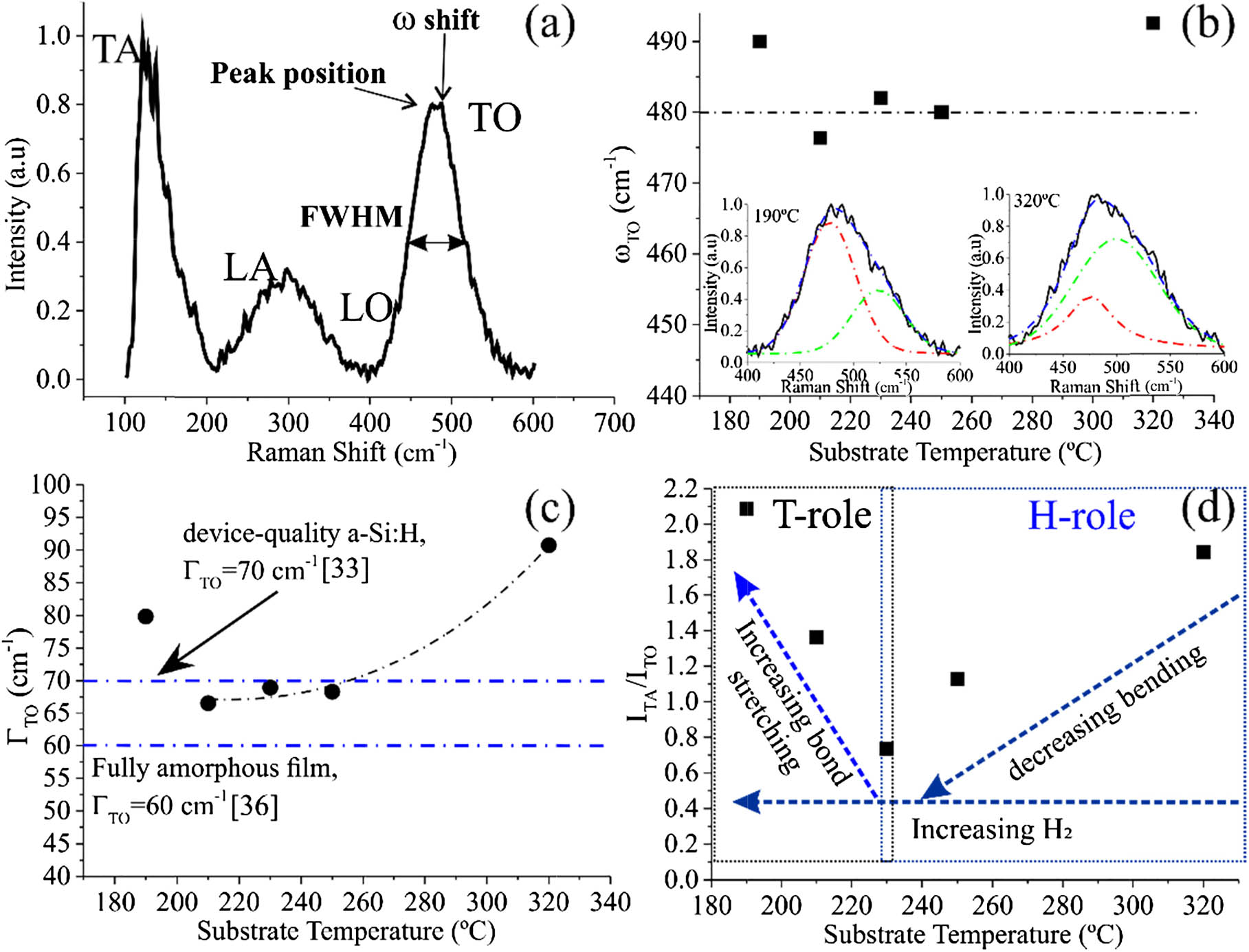
    Fig. 1. Extensive Raman characterization on the structural disorder of an a-Si:H network as a function of Tsub. (a) The Raman spectrum of an a-Si:H network deposited at 230°C of Tsub shows four Raman active modes and the structural information available from those, such as peak position, can indicate chemical species and symmetry; the ω shift can specify the stress and strain; and the FWHM can express the structural disorder and angular distortion of the material network. (b) TO peak position as a function of Tsub, where the dotted line is a guideline for standard TO peak frequency, ωTO of a-Si:H at 480  cm1. Insets are the deconvolution of the TO peak into amorphous and micro-voids in the topology of a-Si:H deposited at 190°C and 320°C, where the solid line represents the TO peak of the Si-Si stretching mode of the deposited film and the dotted lines represent the Gaussian deconvolution of the TO peak. Red dotted lines suggest amorphous and green dotted lines suggest micro-voids. (c) TO peak width ΓTO as a function of Tsub, where dotted lines are guidelines for standard ΓTO at the fully amorphous condition and device-quality a-Si:H. (d) Dependence of the ratio of ITA to ITO on the hydrogen concentration in the diffusion control region. Schematic blue dotted arrows represent how bending modes vary with the hydrogen content in the H-role region and how the stretching mode changes with Tsub in the T-role region.
    (a) An Arrhenius plot shows the deposition rate versus the temperature (square symbol) and shows the propagation loss (dB/cm) corresponding to the deposited temperature (diamond symbol). (b) Cross-sectional SEM images of the a-Si:H films deposited at the different substrate temperatures. The red boxes represent the a-Si:H layer surrounded by silicon dioxide. Inset: the field intensity profile of the propagation mode (at λ=1.55 μm) obtained from the 2 μm width waveguide.
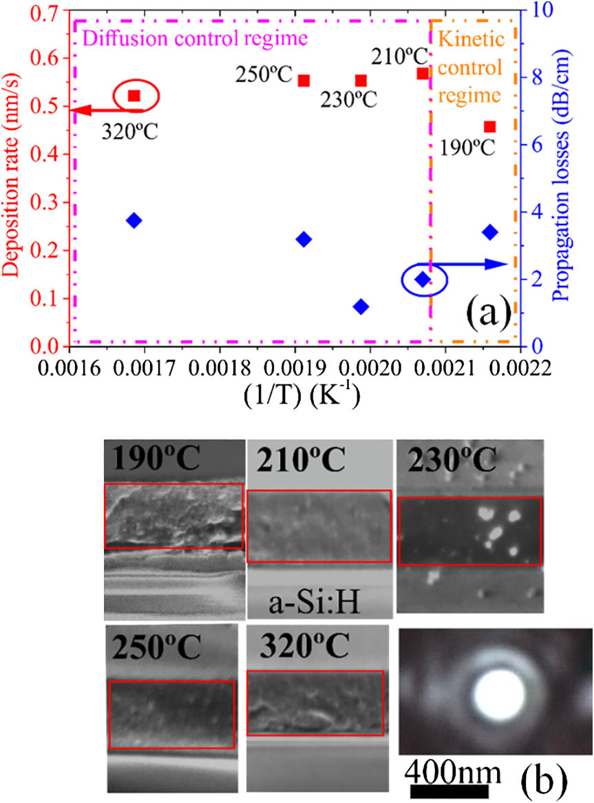
    Fig. 2. (a) An Arrhenius plot shows the deposition rate versus the temperature (square symbol) and shows the propagation loss (dB/cm) corresponding to the deposited temperature (diamond symbol). (b) Cross-sectional SEM images of the a-Si:H films deposited at the different substrate temperatures. The red boxes represent the a-Si:H layer surrounded by silicon dioxide. Inset: the field intensity profile of the propagation mode (at λ=1.55  μm) obtained from the 2 μm width waveguide.
    (a) Measured propagation loss, which is normalized to the coupling loss for different widths. (b) Measured propagation loss (black dots) (dB/cm) of the fully etched ridge waveguide as a function of waveguide width at excitation wavelength 1550 nm. The dotted line is for the eye guide. The squares are the analytically calculated propagation losses. Inset is the cross-sectional image of the measured waveguide, W=350 nm, H=400 nm.
    Fig. 3. (a) Measured propagation loss, which is normalized to the coupling loss for different widths. (b) Measured propagation loss (black dots) (dB/cm) of the fully etched ridge waveguide as a function of waveguide width at excitation wavelength 1550 nm. The dotted line is for the eye guide. The squares are the analytically calculated propagation losses. Inset is the cross-sectional image of the measured waveguide, W=350  nm, H=400  nm.
    (a) AFM images of the surface roughness of a-Si:H deposited at 230°C and 320°C. (b) 2D electric field profiles across the different waveguide widths, where all experimental defects [extinction coefficient, sidewall, surface roughness, air void (as shown in inset of Fig. 3(b)] are counted.
    Fig. 4. (a) AFM images of the surface roughness of a-Si:H deposited at 230°C and 320°C. (b) 2D electric field profiles across the different waveguide widths, where all experimental defects [extinction coefficient, sidewall, surface roughness, air void (as shown in inset of Fig. 3(b)] are counted.
    ReferenceMaterialDeposition MethodDeposited Temperature (°C)Propagation Loss (dB/cm)TypeDimension (W×H)(nm×nm)Etched Depth (nm)Upper CladdingRemark
    [5]a-Si:HPECVD2200.7Rib15×30001200Airλ=1310  nm, without post processing
    [6]a-Si:HPECVD3002Rib1100×1300380Airλ=1550  nm, without post processing
    [7]a-SiPECVD2.7Wire700×100100SiO2λ=1550  nm, 10 nm SiNx intercladding and nitrogen/argon plasma treatment
    [8]a-Si:HPECVD3003.46Wire480×220220SiO2λ=1550  nm, CMPb process on lower cladding
    a-Si:HPECVD3001.34Ridge480×22070
    [9]a-Si:HPECVD4003.2Wire550×220220SiO2λ=1550  nm, CMPb process on lower cladding
    [10]a-SiPECVD3003.8Wire450×220220TEOSaλ=1550  nm, without post processing
    [11]a-Si:HPECVD250-3002Rib2100×2100900SiO2λ=1550  nm, without post processing
    a-Si:HPECVD250-3005.3Wire500×200200
    [12]a-Si:HPECVD2500.6Ridge780×440100TEOSaλ=1550  nm, CMPb process on deposited a-Si:H
    [20]c-Si3.6Strip445×220220Airλ=1550  nm, without post processing
    [21]c-Si3.4Wire630×220220Airλ=1550  nm, sidewall smoothing by wet chemical oxidation
    [22]c-Si0.92Wire500×265265Airλ=1550  nm, without post processing
    This worka-Si:HHWCVD2300.8Wire650×400400SiO2λ=1550  nm, without post processing
    Table 1. Summary of the Performance of a-Si Waveguides and Techniques Used in Silicon Photonics Applications
    Substrate Temperature, Tsub (ºC)ωTO (cm1)ΓTO (cm1)Δθb (°)ITA/ITODeposition Rate (nm/s)Surface Roughness (nm)
    19049079.8510.812.080.461.32
    210476.3666.58.581.360.571.1
    230480.568.98.980.730.551
    25048068.258.881.120.550.84
    320492.690.7812.631.840.523.58
    Table 2. Raman Spectral Information of an a-Si:H Network for Different Substrate Temperatures
    Swe Z. Oo, Antulio Tarazona, Ali Z. Khokhar, Rafidah Petra, Yohann Franz, Goran Z. Mashanovich, Graham T. Reed, Anna C. Peacock, Harold M. H. Chong. Hot-wire chemical vapor deposition low-loss hydrogenated amorphous silicon waveguides for silicon photonic devices[J]. Photonics Research, 2019, 7(2): 193
    Download Citation