Swe Z. Oo1,2,*, Antulio Tarazona2, Ali Z. Khokhar2, Rafidah Petra1..., Yohann Franz2, Goran Z. Mashanovich2, Graham T. Reed2,3, Anna C. Peacock2 and Harold M. H. Chong1|Show fewer author(s)
Abstract
We demonstrate low-loss hydrogenated amorphous silicon (a-Si:H) waveguides by hot-wire chemical vapor deposition (HWCVD). The effect of hydrogenation in a-Si at different deposition temperatures has been investigated and analyzed by Raman spectroscopy. We obtained an optical quality a-Si:H waveguide deposited at 230°C that has a strong Raman peak shift at , peak width (full width at half-maximum) of , and bond angle deviation of 8.98°. Optical transmission measurement shows a low propagation loss of 0.8 dB/cm at the 1550 nm wavelength, which is the first, to our knowledge, report for a HWCVD a-Si:H waveguide.1. INTRODUCTION
Silicon photonics devices are fast evolving from discrete optical components to complete circuits that will eventually require low-loss waveguide interconnects and devices for high-density integration. The reliance of a silicon-on-insulator (SOI) platform for building up active optical devices limits the fabrication freedom in terms of process temperature for the formation of a multilayer photonics platform. Therefore, low temperature deposition of low-loss optical materials is essential for building high-density optical integrated circuits. There have been a variety of low temperature deposition techniques for optical waveguide materials. For example, the use of polymer waveguides is constrained to the uppermost optical layer because of its incompatibility with the CMOS thermal processes [1,2]. Low temperature plasma enhanced chemical vapor deposition (PECVD) materials such as silica- and nitride-based waveguides have been demonstrated. These materials can achieve low propagation losses, but their low refractive indices ( and at 1.55 μm, respectively) require mode matching to the silicon devices, adding a layer of complexity to the design and fabrication. In addition, silicon oxynitride and silicon nitride contain N-H stretching bonds from using ammonia in the deposition processes, which can cause absorption in the s- and c-band wavelength range. Although the N-H bonds can be annealed out at high temperatures close to 1000°C, such processing renders these materials unsuitable for back end of the line (BEOL) processes [3,4].
Hydrogenated amorphous silicon (a-Si:H) waveguides fabricated by the conventional deposition method (PECVD) have been investigated [5–12]. Their low refractive index difference compared with crystalline SOI waveguide devices simplifies integration, especially in multilayer photonics. The waveguide losses in a-Si:H can be investigated from the perspective of its lattice network, which affects absorption in the material. In crystalline silicon (c-Si), the tetrahedral lattice structure has a bond angle of 109.5° and a bond length of 2.35 Å (1 Å = 0.1 nm). The amorphous silicon lattice network comprises 5% and 10% deviation from the crystalline in the bond angle and bond length, respectively [13]. These deviations in amorphous structure do not affect the first few neighboring atoms, which is also known as the short range order (SRO) of an a-Si network. However, the amorphous disorder can induce structural stress to the intermediate range order (IRO; that is, beyond the neighboring atoms in the network), leading to bond breakage and the occurrence of dangling bonds. This has a negative impact on the optoelectronic properties of the a-Si waveguide material, which will suffer from high absorption and degradation over time. Therefore, hydrogen passivation is crucial during or after the deposition of amorphous silicon for the development of waveguide device applications.
There has been a lot of research carried out on different types of deposition and hydrogenation methods for a-Si:H material, such as sputtering, evaporation, glow discharge plasma chemical vapor deposition, PECVD, and catalytic chemical vapor deposition (Cat-CVD) [14–19]. PECVD has been widely reported for the deposition of a-Si:H waveguides [5–12], and the optical propagation losses are summarized and compared to this work in Table 1. Hot-wire chemical vapor deposition (HWCVD), also known as Cat-CVD, has been used to deposit a-Si:H, micro-crystalline silicon (μc-Si:H), and polycrystalline silicon for photovoltaic and thin film transistor applications [23]. Previous work performed by Takahiro et al. [24] demonstrated a waveguide loss of 15 dB/cm at a wavelength of 800 nm. The advantages of HWCVD are its low deposition temperature capability, high deposition rate, no plasma induced damage, and large area homogeneity [25–27]. The complete catalytic and thermal decomposition of the precursor gas silane () is achieved by the hot filament dissociation of Si and four H atoms. In this work, we demonstrate low-loss a-Si:H waveguides for the telecoms wavelength band using the HWCVD process at temperatures compatible with BEOL (below 400°C). Raman spectroscopy was used to analyze the a-Si:H peaks and the amorphous network characteristics due to hydrogenation, thereby correlating its material quality to the waveguide propagation loss at the 1550 nm wavelength. Optical propagation losses were measured using the cut-back method, and control samples with 2 μm wide waveguides were used to initially evaluate the optical propagation characteristics. Sub-micrometer wire waveguides were then fabricated, and a propagation loss of 0.8 dB/cm has been obtained.
Sign up for Photonics Research TOC. Get the latest issue of Photonics Research delivered right to you!Sign up now
| Reference | Material | Deposition Method | Deposited Temperature (°C) | Propagation Loss (dB/cm) | Type | Dimension (W×H)(nm×nm) | Etched Depth (nm) | Upper Cladding | Remark |
| [5] | a-Si:H | PECVD | 220 | 0.7 | Rib | 15×3000 | 1200 | Air | λ=1310 nm, without post processing |
| [6] | a-Si:H | PECVD | 300 | 2 | Rib | 1100×1300 | 380 | Air | λ=1550 nm, without post processing |
| [7] | a-Si | PECVD | — | 2.7 | Wire | 700×100 | 100 | SiO2 | λ=1550 nm, 10 nm SiNx intercladding and nitrogen/argon plasma treatment |
| [8] | a-Si:H | PECVD | 300 | 3.46 | Wire | 480×220 | 220 | SiO2 | λ=1550 nm, CMPb process on lower cladding |
| a-Si:H | PECVD | 300 | 1.34 | Ridge | 480×220 | 70 |
| [9] | a-Si:H | PECVD | 400 | 3.2 | Wire | 550×220 | 220 | SiO2 | λ=1550 nm, CMPb process on lower cladding |
| [10] | a-Si | PECVD | 300 | 3.8 | Wire | 450×220 | 220 | TEOSa | λ=1550 nm, without post processing |
| [11] | a-Si:H | PECVD | 250-300 | 2 | Rib | 2100×2100 | 900 | SiO2 | λ=1550 nm, without post processing |
| a-Si:H | PECVD | 250-300 | 5.3 | Wire | 500×200 | 200 |
| [12] | a-Si:H | PECVD | 250 | 0.6 | Ridge | 780×440 | 100 | TEOSa | λ=1550 nm, CMPb process on deposited a-Si:H |
| [20] | c-Si | — | — | 3.6 | Strip | 445×220 | 220 | Air | λ=1550 nm, without post processing |
| [21] | c-Si | — | — | 3.4 | Wire | 630×220 | 220 | Air | λ=1550 nm, sidewall smoothing by wet chemical oxidation |
| [22] | c-Si | — | — | 0.92 | Wire | 500×265 | 265 | Air | λ=1550 nm, without post processing |
| This work | a-Si:H | HWCVD | 230 | 0.8 | Wire | 650×400 | 400 | SiO2 | λ=1550 nm, without post processing |
Table 1. Summary of the Performance of a-Si Waveguides and Techniques Used in Silicon Photonics Applications
2. SAMPLE PREPARATION
The fabrication process started with thermal oxidation of a p-type Si substrate to produce a 4.6 μm thick cladding, followed by HWCVD of a-Si:H layer on top of the oxide layer. The thick was for optical isolation and to emulate the buried oxide (BOX) of a SOI wafer. The a-Si:H samples used in this work were prepared with the Nitor 301 HWCVD system from ECHERKON Technologies Ltd. The system used 15 tungsten filaments mounted parallel to each other with 2 cm separation. Each filament has a length of 30 cm with diameter variations from 0.125 to 0.2 mm. The different filament wire diameters provide thermal heating to the substrate temperature () ranging from 190°C to 320°C. The reason for using tungsten filaments is their good catalytic performance, low activation energy ( at filament temperature, [28]) for silicon, low cost, and that they are readily available. The distance from the substrate to the filaments was maintained at 6 cm. The system used a constant of 1850°C, which is high enough to achieve the complete dissociation of silane [29,30]. In order to maintain the control of film thickness, the substrate is first pre-heated without introducing any gases. By using different filament diameters, it is possible to obtain different film thickness. The a-Si:H thickness is 400 nm deposited at 0.01 mbar (1 bar = 100 kPa) with a silane and hydrogen gas mix ratio of . The 400 nm thickness is chosen so that the Raman laser (wavelength) penetration depth can fully interrogate the deposited a-Si:H film without interference from the background silicon dioxide layer. After the a-Si:H deposition, the film was covered with 5 nm thick PECVD at 350°C as a passivation layer to prevent atmospheric degradation. We prepared two batches of a-Si:H waveguides. The first batch was fabricated by standard photolithography and anisotropic inductively coupled plasma (ICP) etching to produce 2 μm wide, fully etched wire waveguides, which were used as control samples to study the role of hydrogen in the structural ordering and to correlate this to the optical propagation loss. The second batch was fabricated by direct write lithography and anisotropic ICP etching to produce fully etched wire waveguides with widths of 250, 350, 550, 650, and 850 nm. For each width in batch two, waveguides with different lengths ranging from 3 to 10 mm were produced with grating couplers. Finally, the a-Si:H waveguides were clad with a 1 μm thick PECVD layer.
3. MEASUREMENT SYSTEMS
There are other measurement and characterization techniques such as electron spin resonance (ESR) and the constant photocurrent method (CPM) to evaluate the defects of amorphous silicon [12,31]. These are the viable methods to evaluate absorption in a-Si. In this work, however, we used Raman spectroscopy to evaluate the atomic structure to understand the crystallinity and density of the material. A Renishaw Invia Raman spectrometer with a 532 nm Nd:YAG excitation laser was used. The laser has a penetration depth of 100 nm for a-Si:H material. A scanning electron microscope (SEM) and an atomic force microscope (AFM) were used to examine the cross section and surface roughness of the waveguide. Based on the analysis of the Raman spectra, the best Gaussian fit of a-Si:H network material with optimal was determined. Preliminary transmission measurements were then conducted on the a-Si:H waveguides deposited at various , with dimensions of 2 μm width and 400 nm height, using the Fabry–Perot [32] method to correlate with the Raman results. The light was coupled into the device by the end-fire coupling approach with a magnification objective lens at the input and output of the waveguide. The output light was fed to an InGaAs photodetector. Using the optimized material, wire waveguides with a range of widths were fabricated to evaluate its optical propagation losses. The propagation losses were measured by using the cut-back method with the fiber grating couplers with a total insertion loss of 3 dB, and the optical transmission was normalized to the grating couplers. Agilent 8163B, an integrated tunable laser source, and a photodetector system were used to couple light in and out of the waveguides by gratings and TE polarized optical fibers.
4. MATERIAL CHARACTERIZATION DISCUSSION
Raman spectroscopy has been used for atomic structural characterization of a-Si:H [33,34]. The Raman spectrum of standard a-Si:H has four Raman active phonon modes, namely, a transverse acoustic (TA) peak at , a longitudinal acoustic (LA) peak at , a longitudinal optical (LO) peak at , and a transverse optical (TO) peak at , which can be used to determine the structural quality of a-Si:H [35]. Due to the symmetry in the face centered cubic (fcc) lattice, c-Si has a narrow sharp Raman peak from the TO phonon mode , positioned at , with a full width at half-maximum (FWHM) of about [35]. In amorphous silicon, the small change in the structural distortion of the SRO network induces substantial modification to the phonon density of states. Thus, there is no translation symmetry, and has a broad Raman peak positioned near , with [36,37]. Structural distortion also induces a change in bond length and bond angle . In the Raman spectrum of the amorphous silicon network, the TO phonon (vibration) mode is attributed to the SRO, while the TA, LA, and LO phonon vibration modes are from the structural distortion in the IRO network [34]. Moreover, the area intensity ratio of , , and are sensitive to the change in bond angle of the a-Si network and also indicates structural disorder in the IRO.
Figure 1 shows the Raman shift results from the effect of the deposited temperatures and the structural behavior of the a-Si:H. Figure 1(a) presents the Raman spectrum of a-Si:H material deposited at 230°C, in which all vibration modes are defined. Figure 1(b) provides the Raman shift of as a function of , where the dotted line is a guideline for the center of the Raman line . The plot shows that does not depend on the from 190°C to 320°C as compared to PECVD [34]. The results indicate two regimes for the HWCVD, namely, the diffusion control regime and kinetic control regime indicated in Fig. 2(a), where hydrogenation influences the a-Si:H quality during deposition. It has been shown that the concentration of hydrogen increases with a decrease of in HWCVD [38]. In our experiment, the change of was achieved by changing the diameter of the tungsten filaments. This could induce the additional change in hydrogen concentration, even though the flow rate of the precursors and filament temperature were maintained. It appears there is an interplay of the two mechanisms due to hydrogen and during the deposition process. The a-Si:H material deposited at 210°C, 230°C, and 250°C shows a low structural disorder of the amorphous network with appearing around , which indicates high-quality a-Si:H deposited in this temperature range. It also suggests that hydrogen passivation into the dangling bonds stabilizes the SRO of a-Si. For a-Si:H material deposited at 190°C and 320°C, there is an upshift in to and , respectively, as shown in Fig. 1(b). This is due to the mixture of micro- and nano-scale voids in the amorphous silicon network [33,39,40]. As shown in the inset of Fig. 1(b), the deconvolution of the amorphous peak into two Gaussian functions is related to the amorphous and intermediate voids.
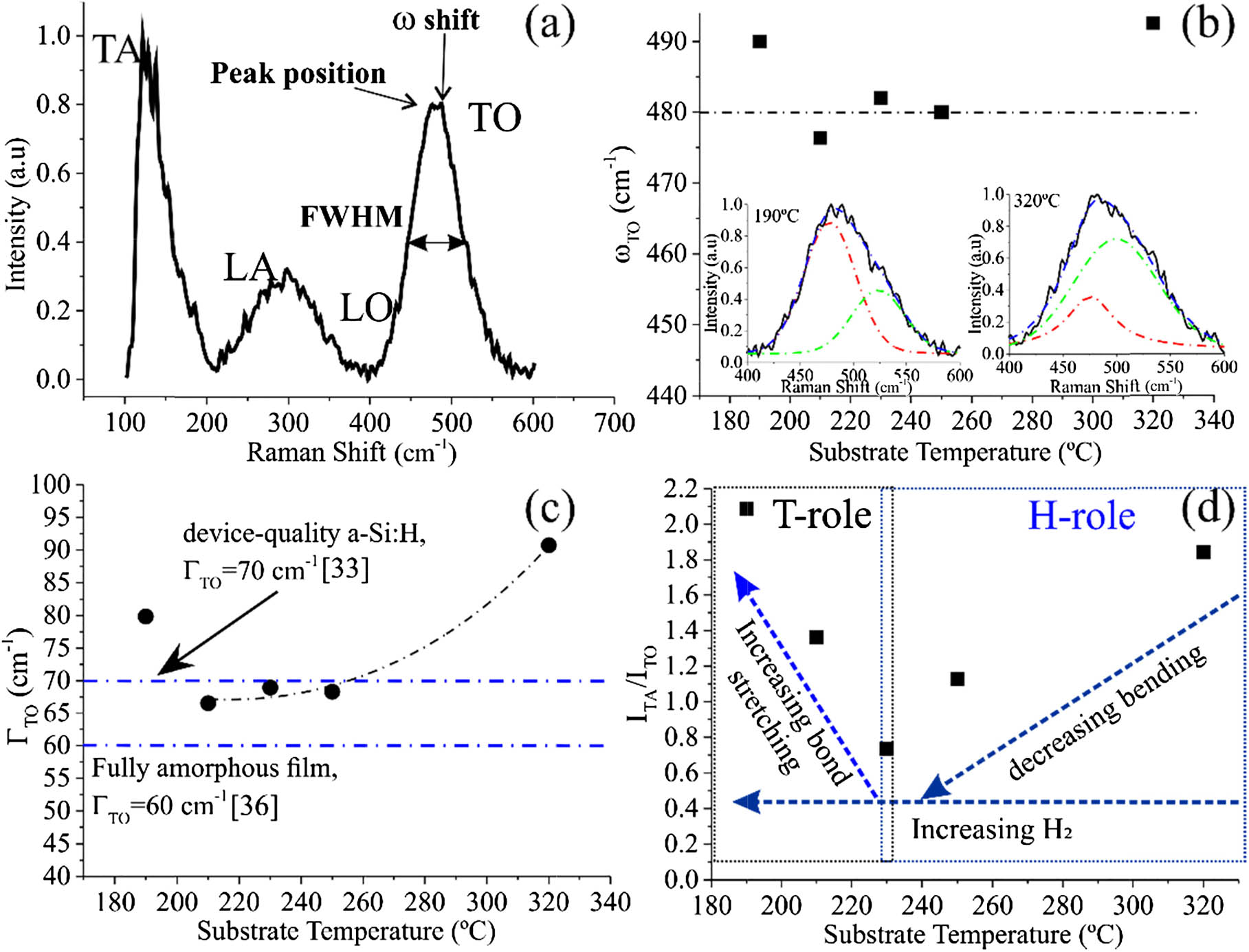
Figure 1.Extensive Raman characterization on the structural disorder of an a-Si:H network as a function of . (a) The Raman spectrum of an a-Si:H network deposited at 230°C of shows four Raman active modes and the structural information available from those, such as peak position, can indicate chemical species and symmetry; the shift can specify the stress and strain; and the FWHM can express the structural disorder and angular distortion of the material network. (b) TO peak position as a function of , where the dotted line is a guideline for standard TO peak frequency, of a-Si:H at . Insets are the deconvolution of the TO peak into amorphous and micro-voids in the topology of a-Si:H deposited at 190°C and 320°C, where the solid line represents the TO peak of the Si-Si stretching mode of the deposited film and the dotted lines represent the Gaussian deconvolution of the TO peak. Red dotted lines suggest amorphous and green dotted lines suggest micro-voids. (c) TO peak width as a function of , where dotted lines are guidelines for standard at the fully amorphous condition and device-quality a-Si:H. (d) Dependence of the ratio of to on the hydrogen concentration in the diffusion control region. Schematic blue dotted arrows represent how bending modes vary with the hydrogen content in the H-role region and how the stretching mode changes with in the T-role region.

Figure 2.(a) An Arrhenius plot shows the deposition rate versus the temperature (square symbol) and shows the propagation loss (dB/cm) corresponding to the deposited temperature (diamond symbol). (b) Cross-sectional SEM images of the a-Si:H films deposited at the different substrate temperatures. The red boxes represent the a-Si:H layer surrounded by silicon dioxide. Inset: the field intensity profile of the propagation mode (at ) obtained from the 2 μm width waveguide.
In the Arrhenius plot of Fig. 2(a), at 320°C of the diffusion control regime, the hydrogen concentration in a-Si:H is expected to be less for the passivation of dangling bonds than in the one deposited at 190°C, which has a reduced densified layer with micro/nano-scale voids and increased average bond length of Si-Si atoms. These a-Si:H films with voids will have an inhomogeneous strain, which translates to a broadening of the peak, as reported by Hishikawa et al. [34], showing a shift in is due to the change in the stretching force of Si-Si bonds in the SRO. For the presence of the Si-H and stretching modes, we managed to obtain broad Raman shift spectra between and (not shown) for the 190°C, 230°C, and 320°C samples. When these spectra were fitted with the Voigt function, we obtained low to medium stretching modes of , , and for the respective deposition temperatures of 190°C, 230°C, and 320°C. The Raman shifts of the 230°C and 320°C samples are the closest to the Si-H bond at , which indicates hydrogenation of the a-Si lattice network. Our measurement agrees with Johnson et al. [41], Matsumura [42], and Smets et al. [43], whose a-Si:H also has a broad Raman peak, showing evidence of Si-H and bonds and also suggesting nano-crystalline and voids in the amorphous silicon network [44]. However, for further verification of Si-H and bonds in a-Si network, Fourier-transform infrared spectroscopy (FTIR) could provide more information of the hydrogen content in the material.
The peak position of TO also indicates the effect of stress in the film, where tensile stress downshifts and compressive stress upshifts . Ratnayake et al. [45] suggest that there is a linear relationship for the internal tensile and compressive stress with regard to the deposition temperature. The film deposited at 210°C shows evidence of tensile stress with a downshift to , while the film deposited at 320°C indicates compressive stress with an upshift to . The Raman spectral information for a-Si:H networks deposited at different , at different deposition rates, and with different surface roughnesses is tabulated in Table 2.
| Substrate Temperature, Tsub (ºC) | ωTO (cm−1) | ΓTO (cm−1) | Δθb (°) | ITA/ITO | Deposition Rate (nm/s) | Surface Roughness (nm) |
| 190 | 490 | 79.85 | 10.81 | 2.08 | 0.46 | 1.32 |
| 210 | 476.36 | 66.5 | 8.58 | 1.36 | 0.57 | 1.1 |
| 230 | 480.5 | 68.9 | 8.98 | 0.73 | 0.55 | 1 |
| 250 | 480 | 68.25 | 8.88 | 1.12 | 0.55 | 0.84 |
| 320 | 492.6 | 90.78 | 12.63 | 1.84 | 0.52 | 3.58 |
Table 2. Raman Spectral Information of an a-Si:H Network for Different Substrate Temperatures
The FWHM width of the TO peak () is proportional to the structural angular distortion, which means the larger the , the more structural distortion in the bond angle distribution [36]. Figure 1(c) shows the dependence of structural deformation on the substrate temperature . The material deposited at 210°C has an FWHM of compared to the pure amorphous Si, which has a of . Han et al. [33] reported that device-quality a-Si:H has a centered at with FWHM of , which closely matches our experimental result at with at for the a:Si-H material deposited at 230°C. Based on Beeman’s linear relationship [36] () between and bond angle deviation , the a-Si:H material deposited at 230°C has a bond angle deviation of 8.98°, with respect to the crystalline Si bond angle. Our bond angle deviation result is within the range reported by Beeman et al. and Han et al. on a fully formed amorphous silicon network [33,36]. The FWHM becomes wider when is at 190°C and 320°C (shown in Table 2), which implies changes in inter-atomic lattice spacing due to either compressive or tensile strain and thus larger bond angle fluctuations. The exact bond angle fluctuation requires future X-ray diffraction measurements and correlates to and with a that requires more temperature points. For now, our goal is to achieve low temperature deposition of a-Si:H for silicon photonics applications.
The TA phonon mode at the Raman peak position of is attributed to the bond bending mode in the IRO of the amorphous network, while the TO phonon at is attributed to the bond stretching mode in the SRO of the amorphous network [38]. By taking the Raman area intensity ratio of peak to peak, we can study the role of hydrogen on the TA bending modes (IRO) and TO stretching modes (SRO). Figure 1(d) presents information related to the role of hydrogen on the IRO or SRO. In the hydrogen-dominated diffusion control regime, bond bending decreases [] as the hydrogen concentration increases, which indicates that the effect of hydrogen on the structural disorder is more prominent in the IRO than in the SRO. This observation matches the experimental results of Gupta et al. [38]. In the temperature ()-governed kinetic control regime, bond stretching increases with decreasing , indicating that thermally induced structural distortion is more obvious in the SRO. These results show a balance between hydrogen diffusion and thermal deposition required to achieve device-quality a-Si:H. The experiments also show the optimized temperature of 230°C, which meets the above requirement.
The cross-section SEM images of the a-Si:H films are shown in Fig. 2(b), where the red box highlights the core thickness of 400 nm surrounded by . The films deposited at 190°C and 320°C show granular structure due to defects such as microvoids. The a-Si:H film deposited at 230°C is relatively defect free with high densification. The small particles on the facets are due to residue from the cleaving.
5. RESULTS AND DISCUSSION
Initial propagation loss measurements were performed with the Fabry–Perot method on the 2 μm wide fully etched waveguides deposited at different temperatures. Figure 2(a) shows the deposition rate and the propagation loss of the a-Si:H waveguide for the different temperatures. The mass transport control (also known as diffusion control) deposition regime is observed at temperatures above 210°C, which is characterized by small changes of the deposition rate with temperature. The surface-limited or kinetic control regime occurs below 200°C, where the deposition rate is dependent on temperature changes. The small drop in the deposition rate at 320°C could also suggest that gas reactions are more prominent above this temperature, but temperatures above this point were not investigated as they are outside the temperature range of interest. The average deposition rate of a-Si:H material is 0.55 nm/s for the temperature range 210°C–320°C, while the deposition rate drops to 0.45 nm/s at of 190°C. It is noteworthy that the trend in the Raman shift matches the trend in the propagation loss measurements, where the loss of a-Si:H deposited at 190°C and 320°C is higher compared to those of a-Si:H at 210°C, 230°C, and 250°C. The waveguide deposited at 230°C gives the lowest loss of 1 dB/cm. The inset in Fig. 2(b) shows the optical intensity profile from the end facet of the waveguide. We note that the AFM root mean square (rms) surface roughness of the a-Si:H film deposited at 190°C and 320°C is 1.32 nm and 3.58 nm, respectively, while the a-Si:H deposited at 210°C, 230°C, and 250°C has an rms roughness of about 1 nm (see Table 2).
From the Raman characterization, the a-Si:H film deposited at of 230°C is a promising candidate for low-loss silicon photonics platforms. Therefore, a 400 nm thick a-Si:H film was deposited at 230°C, wire waveguides with different widths were fabricated as mentioned in Section 2, with their propagation losses assessed by the cut-back method, and coupling with optical fibers was performed via grating couplers. The ellipsometer measurement showed that refractive index , , and estimated band gap energy were measured for the bulk material at 1550 nm using the Cody–Lorentz model [46].
The measured propagation losses at a wavelength of 1550 nm for different widths are shown in Fig. 3(a). The cross-section image of a waveguide with a width of 350 nm is shown in the inset of Fig. 3(b). Waveguides with widths ranging from 350 to 850 nm were measured under TE polarization, while the narrow 250 nm wide waveguide was measured under TM polarization only. The propagation loss [decibels per centimeter (dB/cm)] as a function of waveguide width is plotted in Fig. 3(b). The propagation loss was decreased with increasing width. The lowest propagation loss is 0.8 dB/cm for the 650 nm wide waveguide, while the 350 nm wide waveguide has a loss of 27 dB/cm. The higher loss is due to the weaker optical confinement and mode interaction with the surrounding sidewall roughness and air voids as seen in the inset of Fig. 3(b). For an 850 nm wide waveguide, the loss was increased to 3 dB/cm, which could be attributed to the fabrication error. Since the optical confinement is well within the 650 nm wide waveguide, and as the rms surface roughness is low, we focused our analysis on how much material absorption contributes to the loss after the hydrogenation and deposition at 230°C. The extinction coefficient κ can be calculated using the measured loss as the absorption coefficient , where . Using the excitation wavelength at 1550 nm, the extinction coefficient is .
Figure 3.(a) Measured propagation loss, which is normalized to the coupling loss for different widths. (b) Measured propagation loss (black dots) (dB/cm) of the fully etched ridge waveguide as a function of waveguide width at excitation wavelength 1550 nm. The dotted line is for the eye guide. The squares are the analytically calculated propagation losses. Inset is the cross-sectional image of the measured waveguide, , .
To evaluate the origin of the losses, we performed numerical analysis using a commercial software called MODE Solutions by Lumerical that uses a finite-difference eigenmode (FDE) solver approach to calculate the loss. We modeled all fabricated widths of the wire waveguides in the following order: (a) with absorption but without roughness and (b) with an absorption coefficient, sidewall/surface roughness, and air voids, which are artifacts from fabrication. Simulations for different waveguide widths were executed using the and values from the ellipsometer. First, the extinction coefficient was added into the material to simulate the propagation loss of the waveguide due to the material absorption at the 1550 nm wavelength. The extracted extinction coefficient is , which closely matched our analytical estimate of . Under the assumption of high optical confinement, the simulated loss of 0.73 dB/cm is comparable to the experimental loss of 0.8 dB/cm for the 650 nm wide waveguide. Further simulation with only the extinction coefficient on other waveguide widths shows no significant changes in the propagation loss. AFM measurement of surface roughness is shown in Fig. 4(a). From the cross-sectional view of the waveguide [inset of Fig. 3(b)], air voids are present between the cladding and the a-Si:H waveguide. All these roughness factors were taken into account in simulation condition (b). The sidewall of waveguide has the anisotropic roughness (7 nm correlation length) to resemble the etching result, while the AFM measured top and bottom surface roughness is 3.58 nm (worst case). The same sidewall roughness was applied to the air void, where the width of the air void is 50 nm at an angle of 30° to emulate the fabricated features shown in Fig. 3(b). All waveguides support the fundamental TE mode, except from the waveguide that has 250 nm width, as shown in Fig. 4(b). The simulated propagation losses (red squares) were plotted together with the experimental loss (black dots) in Fig. 3(b). The simulation and the experimental results show excellent agreement, which strongly suggests that roughness scattering dominates the propagation loss more than the material absorption. This means the HWCVD a-Si:H deposited at 230°C has very good hydrogen passivation in the SRO amorphous network.
Figure 4.(a) AFM images of the surface roughness of a-Si:H deposited at 230°C and 320°C. (b) 2D electric field profiles across the different waveguide widths, where all experimental defects [extinction coefficient, sidewall, surface roughness, air void (as shown in inset of Fig. 3(b)] are counted.
6. CONCLUSION
From the Raman results, in addition to an a-Si:H Raman shift of , it is critical to achieve an FWHM of less than and a bond angle deviation of . This is to ensure the optical quality of a-Si:H material for waveguide device applications. We have achieved those conditions at a deposition temperature of 230°C and shown that the absorption loss is lower than the scattering loss. We demonstrated, for the first time to our knowledge, a very low optical loss of 0.8 dB/cm at the 1550 nm wavelength using the HWCVD method. This low-loss waveguide offers a potential interconnect solution for high-density silicon photonics integration.
Acknowledgment
Acknowledgment. The authors thank Southampton Nano Fabrication Centre, University of Southampton. G. T. Reed is a Royal Society Wolfson Merit Award holder. He is grateful to both the Royal Society and the Wolfson Foundation. The authors acknowledge Dr. Antoine F. J. Runge for his help in the optical measurement using the Fabry–Perot method. All authors also thank Dr. David Thomson for letting us use his grating coupler transmission measurement setup.
References
[1] S. K. A. Neyer, E. Rabe, D. Cai. Polymer waveguide technologies for optical interconnects. European Conference on Integrated Optics (ECIO), ThD0(2007).
[2] A. Yeniay, R. Gao, K. Takayama, R. Gao, A. F. Garito. Ultra-low-loss polymer waveguides. J. Lightwave Technol., 22, 154-158(2004).
[3] C. K. Wong, H. Wong, M. Chan, Y. T. Chow, H. P. Chan. Silicon oxynitride integrated waveguide for on-chip optical interconnects applications. Microelectron. Reliab., 48, 212-218(2008).
[4] E. G. Johnson, M. J. Shaw, G. P. Nordin, J. Guo, G. A. Vawter, T. J. Suleski, S. Habermehl, C. T. Sullivan. Fabrication techniques for low-loss silicon nitride waveguides. Proc. SPIE, 5720, 1-11(2005).
[5] G. C. Righini, G. Cocorullo, S. I. Najafi, F. G. Della Corte, R. De Rosa, B. Jalali, I. Rendina, A. Rubino, E. Terzini. Amorphous silicon waveguides and interferometers for low-cost silicon optoelectronics. Proc. SPIE, 3278, 286-292(1998).
[6] A. Harke, M. Krause, J. Mueller. Low-loss single mode amorphous silicon waveguides. Electron. Lett., 41, 1377-1379(2005).
[7] R. Sun, K. McComber, J. Cheng, D. K. Sparacin, M. Beals, J. Michel, L. C. Kimerling. Transparent amorphous silicon channel waveguides with silicon nitride intercladding layer. Appl. Phys. Lett., 94, 141108(2009).
[8] S. K. Selvaraja, E. Sleeckx, M. Schaekers, W. Bogaerts, D. V. Thourhout, P. Dumon, R. Baets. Low-loss amorphous silicon-on-insulator technology for photonic integrated circuitry. Opt. Commun., 282, 1767-1770(2009).
[9] S. Zhu, G. Q. Lo, D. L. Kwong. Low-loss amorphous silicon wire waveguide for integrated photonics: effect of fabrication process and the thermal stability. Opt. Express, 18, 25283-25291(2010).
[10] J. Kang, Y. Atsumi, M. Oda, T. Amemiya, N. Nishiyama, S. Arai. Low-loss amorphous silicon multilayer waveguides vertically stacked on silicon-on-insulator substrate. Jpn. J. Appl. Phys., 50, 120208(2011).
[11] T. Lipka, O. Horn, J. Amthor, J. Müller. Low-loss multilayer compatible a-Si:H optical thin films for photonic applications. JEOS RP, 7, 12033(2012).
[12] R. Takei, S. Manako, E. Omoda, Y. Sakakibara, M. Mori, T. Kamei. Sub-1 dB/cm submicrometer-scale amorphous silicon waveguide for backend on-chip optical interconnect. Opt. Express, 22, 4779-4788(2014).
[13] G. Franco, P. Padmanabhan. Optoelectronic properties of amorphous silicon, the role of hydrogen: from experiment to modeling. Optoeletronics: Materials and Techniques, 496(2011).
[14] T. Karabacak, Y. P. Zhao, G. C. Wang, T. M. Lu. Growth-front roughening in amorphous silicon films by sputtering. Phys. Rev. B, 64, 085323(2001).
[15] M. H. Brodsky, M. Cardona, J. J. Cuomo. Infrared and Raman spectra of the silicon-hydrogen bonds in amorphous silicon prepared by glow discharge and sputtering. Phys. Rev. B, 16, 3556-3571(1977).
[16] Y. Abdulraheem, I. Gordon, T. Bearda, H. Meddeb, J. Poortmans. Optical bandgap of ultra-thin amorphous silicon films deposited on crystalline silicon by PECVD. AIP Adv., 4, 057122(2014).
[17] J. Robertson. Deposition mechanism of hydrogenated amorphous silicon. J. Appl. Phys., 87, 2608-2617(2000).
[18] D. Kaplan, N. Sol, G. Velasco, P. A. Thomas. Hydrogenation of evaporated amorphous silicon films by plasma treatment. Appl. Phys. Lett., 33, 440-442(1978).
[19] H. Matsumura. Catalytic chemical vapor deposition (CTC-CVD) method producing high quality hydrogenated amorphous silicon. Jpn. J. Appl. Phys., 25, L949-L951(1986).
[20] Y. A. Vlasov, S. J. McNab. Losses in single-mode silicon-on-insulator strip waveguides and bends. Opt. Express, 12, 1622-1631(2004).
[21] D. K. Sparacin, S. J. Spector, L. C. Kimerling. Silicon waveguide sidewall smoothing by wet chemical oxidation. J. Lightwave Technol., 23, 2455-2461(2005).
[22] M. Gnan, S. Thoms, D. S. Macintyre, R. M. De La Rue, M. Sorel. Fabrication of low-loss photonic wires in silicon-on-insulator using hydrogen silsesquioxane electron-beam resist. Electron. Lett., 44, 115-116(2008).
[23] R. E. I. Schropp. Hot wire chemical vapor deposition: recent progress, present state of the art and competitive opportunities. ECS Trans., 25, 3-14(2009).
[24] A. Takahiro, I. Makoto, M. Takeo, I. Koichi, O. Keisuke, M. Hideki. Propagation loss of amorphous silicon optical waveguides at the 0.8 μm-wavelength range. 7th IEEE International Conference on Group IV Photonics, 269-271(2010).
[25] R. S. Crandalla, X. Liub, E. Iwaniczkoa. Recent developments in hot wire amorphous silicon. J. Non-Cryst. Solids, 227–230, 23-28(1998).
[26] K. F. Feenstra, R. E. I. Schropp, W. F. Van der Weg. Deposition of amorphous silicon films by hot-wire chemical vapor deposition. J. Appl. Phys., 85, 6843-6852(1999).
[27] A. H. Mahan, J. Carapella, B. P. Nelson, R. S. Crandall, I. Balberg. Deposition of device quality, low H content amorphous silicon. J. Appl. Phys., 69, 6728-6730(1991).
[28] S. Tange, K. Inoue, K. Tonokura, M. Koshi. Catalytic decomposition of SiH4 on a hot filament. Thin Solid Films, 395, 42-46(2001).
[29] K. Tonokura, K. Inoue, M. Koshi. Chemical kinetics for film growth in silicon HWCVD. J. Non-Cryst. Solids, 299–302, 25-29(2002).
[30] Y.-F. Wang, R. Pollard. An approach for modeling surface reaction kinetics in chemical vapor deposition processes. J. Electrochem. Soc., 142, 1712-1725(1995).
[31] T. Shimizu, H. Kidoh, M. Matsumoto, A. Morimoto, M. Kumeda. Photo-created defects in a-Si:H as elucidated by ESR, LESR and CPM. J. Non-Cryst. Solids, 114, 630-632(1989).
[32] S. Taebi, M. Khorasaninejad, S. Singh Saini. Modified Fabry-Perot interferometric method for waveguide loss measurement. Appl. Opt., 47, 6625-6630(2008).
[33] D. Han, J. D. Lorentzen, J. Weinberg-Wolf, L. E. McNeil, Q. Wang. Raman study of thin films of amorphous-to-microcrystalline silicon prepared by hot-wire chemical vapor deposition. J. Appl. Phys., 94, 2930-2936(2003).
[34] Y. Hishikawa, K. Watanabe, S. Tsuda, M. Ohnishi, Y. Kuwano. Raman study on the silicon network of hydrogenated amorphous silicon films deposited by a glow discharge. Jpn. J. Appl. Phys., 24, 385-389(1985).
[35] R. Carius, J. M. Marshall, D. Dimova-Malinovska. Structural and optical properties of microcrystalline silicon for solar cell applications. Photovoltaic and Photoactive Materials: Properties, Technology and Applications, 353(2002).
[36] D. Beeman, R. Tsu, M. F. Thorpe. Structural information from the Raman spectrum of amorphous silicon. Phys. Rev. B, 32, 874-878(1985).
[37] L. Houben, M. Luysberg, P. Hapke, R. Carius, F. Finger, H. Wagner. Structural properties of microcrystalline silicon in the transition from highly crystalline to amorphous growth. Philos. Mag. A, 77, 1447-1460(1998).
[38] S. Gupta, R. S. Katiyar, G. Morell, S. Z. Weisz, I. Balberg. The effect of hydrogen on the network disorder in hydrogenated amorphous silicon. Appl. Phys. Lett., 75, 2803-2805(1999).
[39] Z. Wang, D. Flötotto, E. J. Mittemeijer. Stress originating from nanovoids in hydrogenated amorphous semiconductors. J. Appl. Phys., 121, 095307(2017).
[40] A. H. M. Smets, W. M. M. Kessels, M. C. M. van de Sanden. Vacancies and voids in hydrogenated amorphous silicon. Appl. Phys. Lett., 82, 1547-1549(2003).
[41] E. V. Johnson, L. Kroely, P. Roca i Cabarrocas. Raman scattering analysis of SiH bond stretching modes in hydrogenated microcrystalline silicon for use in thin-film photovoltaics. Solar Energy Mater. Sol. Cells, 93, 1904-1906(2009).
[42] M. Hideki. Formation of silicon-based thin films prepared by catalytic chemical vapor deposition (Cat-CVD) method. Jpn. J. Appl. Phys., 37, 3175-3187(1998).
[43] A. H. M. Smets, T. Matsui, M. Kondo. High-rate deposition of microcrystalline silicon p-i-n solar cells in the high pressure depletion regime. J. Appl. Phys., 104, 034508(2008).
[44] D. Stryahilev, F. Diehl, B. Schröder. The splitting of absorption bands in IR spectra of anisotropic SiH monolayers covering the internal surfaces in μc-Si:H. J. Non-Cryst. Solids, 266–269, 166-170(2000).
[45] D. Ratnayake, M. D. Martin, U. R. Gowrishetty, D. A. Porter, T. A. Berfield, S. P. McNamara, K. M. Walsh. Engineering stress in thin films for the field of bistable MEMS. J. Micromech. Microeng., 25, 125025(2015).
[46] A. S. Ferlauto, G. M. Ferreira, J. M. Pearce, C. R. Wronski, R. W. Collins, X. Deng, G. Ganguly. Analytical model for the optical functions of amorphous semiconductors from the near-infrared to ultraviolet: applications in thin film photovoltaics. J. Appl. Phys., 92, 2424-2436(2002).


