
Guiying Shen, Youwen Zhao, Yongbiao Bai, Jingming Liu, Hui Xie, Zhiyuan Dong, Jun Yang, Ding Yu. Photoluminescene study acceptor defects in lightly doped n type GaSb single crystals[J]. Journal of Semiconductors, 2019, 40(4): 042101
- Journal of Semiconductors
- Vol. 40, Issue 4, 042101 (2019)
Abstract
1. Introduction
Gallium antimonide (GaSb) is an important semiconductor material for fabricating infrared opto-electronic devices and thermophotovoltaic cells. In particular, GaSb substrate has been successfully applied to manufacture type-II InAs/GaSb superlattice infrared detectors operating from mid to long wavelength[
GaSb single crystals can be grown by three methods: the Czochralski technique (CZ), vertical gradient freeze (VGF) and liquid encapsulated Czochralski technique (LEC)[
In this paper, photoluminescence (PL) spectroscopy has been used to study defects in as-grown and lightly Te-doped GaSb single crystals. Special attention is paid to the variations of native acceptor defect with the change of Te-doping concentration and their combined influences on the properties of GaSb.
2. Experiments
(100) GaSb wafers with 750 μm thickness were sliced from lightly Te-doped GaSb bulk single crystal ingots grown by LEC technique. The wafers were polished on both sides for the optical measurement. The electrical properties, including carrier concentration and mobility were investigated through a Hall measurements system at room temperature. The PL spectra of the samples were obtained at 10 K by using a Bruker Vertex 80 FTIR equipped with an InSb detector. The excitation power of the PL spectra was 100 mW.
3. Results and discussion
The electrical parameters of GaSb samples with different Te-doping concentration are listed in Table 1. For n-type GaSb samples, the free carrier concentration varies from 1.66 × 10¹⁶ to 1.38 × 1017 cm−3 and the mobility changes from 2.34 × 10³ to 3.34 × 103 cm2/(V·s). It has been found that the mobility increases with the increasing carrier concentration due to the compensation of Te atoms. The native defects that exist in as-grown GaSb, e.g. VGa and GaSb, have a negative effect on the electron transition process and decrease the mobility. In Te-doped GaSb samples, the Te atoms are very likely to occupy the sites of vacancy defects. Thus, the ionized impurity scatting is suppressed and the mobility will increase with the increasing Te-doping concentration. However, when it turns from sample 6 to 7, the mobility decreases from 3.34 × 10³ to 3.24 × 103 cm2/(V·s), due to the stronger free carrier scatting exists in sample 7. Samples 8 and 9 have p-type conduction with relative low mobility. The low mobility of sample 8, which is prepared as an undoped wafer, can be attributed to the high concentration of native acceptor defects. The mobility of sample 9, which is lightly Te-doped GaSb, is higher than that of sample 8 because of the light degree of compensation of Te atoms. The electrical properties of samples 8 and 9 are listed in Table 1 as a comparison to find the transformation of the defects concentration and properties. The charge-neutrality condition can be written as
where n0 denotes the electron concentration,
i.e. high concentration of native acceptor (VGa and GaSb) exhibits in p-type GaSb. In n-type GaSb, electrons become the main carrier, while the concentration of holes and ionized acceptors can be ignored. Te atoms ionized as donors play a leading role in compensating the native acceptor defects, forming the main ionized acceptors in the structure of VGaTeSb.
Photoluminescene (PL) measurement can be effectively used to study the details of defects in a material. More information about the electron and exciton transitions can be obtained from PL spectra measured at low temperature. It is found that four kinds of absorption process exhibit in GaSb single crystals[
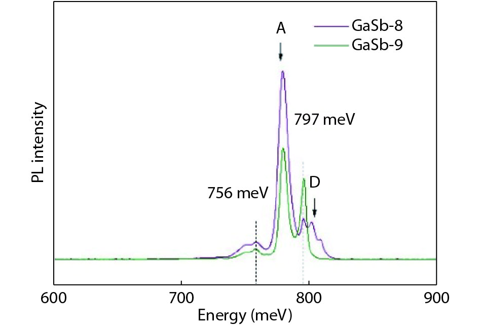
Fig. 1 shows the PL spectra of the p-type GaSb samples. It can be seen that the intensity of the peak A and the peak at 756 meV is lower than that of sample 9. While the intensity of the 797 meV peak increases after doping Te atoms lightly. It has been reported that band A is related to the VGa and the peak at 756 meV is attributed to GaSb, inferring that the VGa and GaSb defects will be restrained by doping with Te atoms. The increasing intensity of the 797 meV peak indicates a decreasing of concentration of native defects[
![]()
Figure 1.(Color online) PL spectra of p-type GaSb samples measured at 10 K.
![]()
Figure 2.(Color online) PL spectra of sample 2 at 10 K.
![]()
Figure 3.(Color online) PL spectra of samples 1, 3 and 4 at 10 K.
In Figs. 2–4, a broad peak with several resolved peaks shows up and it dominates the spectrum of the Te-doped GaSb with the carrier concentration below 1.4 × 1017 cm−3. In the lightly Te doped GaSb samples, the broad band incorporates a new peak, named peak G, around 664 meV, which is related to the complex defects consisting of totally ionized Te atoms and partial compensated native acceptor defects, such as VGa and GaSb. As the doping concentration increases, more native acceptor defects are compensated by the ionized Te atoms. Thus, the PL peak of the complex defects becomes weaker as the Te-doping concentration increases. It is expected that a native acceptor defect will be compensated completely when the doping concentration exceeds the critical value, resulting in annihilation of the complex defects.
![]()
Figure 4.(Color online) PL spectra of samples 5, 6 and 7 at 10 K.
Table 3 shows the position and strength of peaks G, C and T which are resolved from the integrated broaden peak (the resolved peak A and D are not listed due to their weakness). Peak G shows relatively high strength for sample 1 and it then drops rapidly with the increase of Te-doping concentration. Peak G almost disappears, when it turns to sample 6 and 7. The intensity of peak C shows a little increase from sample 1 to 4 and then drops rapidly as the carrier concentration increases. The increase can be explained as the change of occupation state of the residual acceptors which leads to the moving up of Fermi level[
Vlasov has pointed out that the FWHM of peak C is proportional to the defect concentration[
4. Conclusion
The electrical and optical properties of the as-grown and lightly Te-doped GaSb samples have been investigated through Hall measurement and PL spectra. Native acceptor defects are suppressed with the increasing Te-doping concentration. The PL spectra show good correlation between the Te-doping concentration and the intensity of the defect related peaks. In the native acceptor defects GaSb and VGa that are compensated by Te atoms and GaSb related peaks almost totally disappear when VGa defects become the main acceptor defects. A new band around 665 meV appears in the samples with carrier concentration below 7.84 × 1016 cm−3. It can be argued that this band corresponds to the complex defects consisting of ionized Te atom, native acceptor defects VGa and GaSb. More native acceptor defects are compensated by the ionized Te atoms, as the doping concentration increases. It is also found that native acceptor defects are compensated completely when the doping concentration exceeds the critical value, resulting in annihilation of the complex defects.
References
[1] P S Dutta, H L Bhat, V Kumar. The physics and technology of gallium antimonide: An emerging optoelectronic material. J Appl Phys, 81, 5821(1997).
[2] N Zia, J Viheriälä, R Koskinen et al. High power (60 mW) GaSb-based 1.9
[3] X Zhou, D Li, J Huang et al. Mid-wavelength type II InAs/GaSb superlattice infrared focal plane arrays. Infrared Phys Technol, 78, 263(2016).
[4] H J Haugan, G J Brown, F Szmulowicz et al. InAs/GaSb type-II superlattices for high performance mid-infrared detectors. J Cryst Growth, 278, 198(2005).
[5] J Su, T Liu, J M Liu et al. Thermally induced native defect transform in annealed GaSb. Chin Phys B, 25, 077801(2016).
[6] J Kujala, N Segercrantz, F Tuomisto et al. Native point defects in GaSb. J Appl Phys, 116, 143508(2014).
[7] N Segercrantz, J Slotte, I Makkonen et al. Point defect balance in epitaxial GaSb. Appl Phys Lett, 105, 082113(2014).
[8] H A Tahini, A Chroneos, S T Murphy et al. Vacancies and defect levels in III–V semiconductors. J Appl Phys, 114, 063517(2013).
[9] A S Vlasov, E P Rakova, V P Khvostikov et al. Native defect concentration in Czochralski-grown Te-doped GaSb by photoluminescence. Sol Energ Mat Sol C, 94, 1113(2010).
[10] W G Hu, Z Wang, B F Su et al. Gallium antisite defect and residual acceptors in undoped GaSb. Phys Lett A, 332, 286(2004).
[11] P Rudolph, M Czupalla, B Lux. LEC growth of semi-insulating GaAs crystals in traveling magnetic field generated in a heater–magnet module. J Cryst Growth, 311, 4543(2009).
[12] B C Houchens, P Becla, S E Tritchler et al. Crystal growth of bulk ternary semiconductors: comparison of GaInSb growth by horizontal Bridgman and horizontal traveling heater method. J Cryst Growth, 312, 1091(2010).
[13] P G Mo, H Z Tan, L X Du et al. A novel technique for Czochralski growth of GaSb single crystals. J Cryst Growth, 126, 613(1993).
[14] R Pino, Y Ko, P S Dutta. Enhancement of infrared transmission in GaSb bulk crystals by carrier compensation. J Appl Phys, 96, 1064(2004).
[15] Y B Bai, Y W Zhao, G Y Shen et al. N-type GaSb single crystals with high below-band gap transmission. Chin Phys B, 26, 107801(2017).
[16] A Chandola, R Pino, P S Dutta. Below bandgap optical absorption in tellurium-doped GaSb. Semicond Sci Technol, 20, 886(2005).
[17] A Bignazzi, A Bosacchi, R Magnanini. Photoluminescence study of heavy doping effects in Te-doped GaSb. J Appl Phys, 81, 7540(1997).
[18] M C Wu, C C Chen. Photoluminescence of liquid-phase epitaxial Te-doped GaSb. J Appl Phys, 73, 8495(1993).
[19] P S Dutta, K S R K Rao, H L Bhat et al. Photoluminescence studies in bulk gallium antimonide. Appl Phys A, 61, 149(1995).
[20] W J Jiang, Y M Sun, M C Wu. Electrical and photoluminescent properties of high-quality GaSb and AlGaSb layers grown from Sb-rich solutions by liquid-phase epitaxy. J Appl Phys, 77, 1725(1995).

Set citation alerts for the article
Please enter your email address
© Copyright 2018-2021 | Chinese Laser Press. All Rights Reserved 沪ICP备15018463号-20