• Journal of Infrared and Millimeter Waves
  • Vol. 41, Issue 4, 659 (2022)
Meng CAO1、2, Bin YU1, Xiang ZHANG2, Cheng-Gang XU2, Shan ZHANG3, Li-Ying SUN4、*, Xiao-Hong TAN2, Yu-Cheng JIANG5, Jia-Wei DOU2, and Lin-Jun WANG2、6
Author Affiliations
  • 1State Key Laboratory of Nuclear Power Safety Monitoring Technology and Equipment,China Nuclear Power Engineering Co.,Ltd.,Shenzhen 518172,China
  • 2School of Materials Science and Engineering,Shanghai University,Shanghai,200072,China
  • 3Key Laboratory of infrared imaging materials and detectors,Shanghai Institute of Technical Physics,Chinese Academy of Sciences,Shanghai,200083,China
  • 4Intensive Care Unit,Yangpu District Shidong Hospital,,Shanghai 200438,China
  • 5School of Physical Science and Technology,Suzhou University of Science and Technology,Suzhou 215009,China
  • 6Zhejiang Institute of Advanced Materials,SHU,Jiashan314113,China
  • show less
    DOI: 10.11972/j.issn.1001-9014.2022.04.001 Cite this Article
    Meng CAO, Bin YU, Xiang ZHANG, Cheng-Gang XU, Shan ZHANG, Li-Ying SUN, Xiao-Hong TAN, Yu-Cheng JIANG, Jia-Wei DOU, Lin-Jun WANG. Photoelectrochemical properties of sputtered n-type CdTe thin films[J]. Journal of Infrared and Millimeter Waves, 2022, 41(4): 659 Copy Citation Text show less
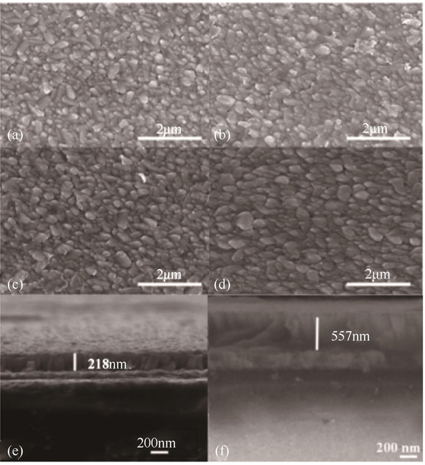
    Surficial and sectional SEM images of n-type CdTe thin film with deposition time(a)15 min,(b)20 min,(c)25 min,(d)30 min,(e)20 min,(f)30 min.
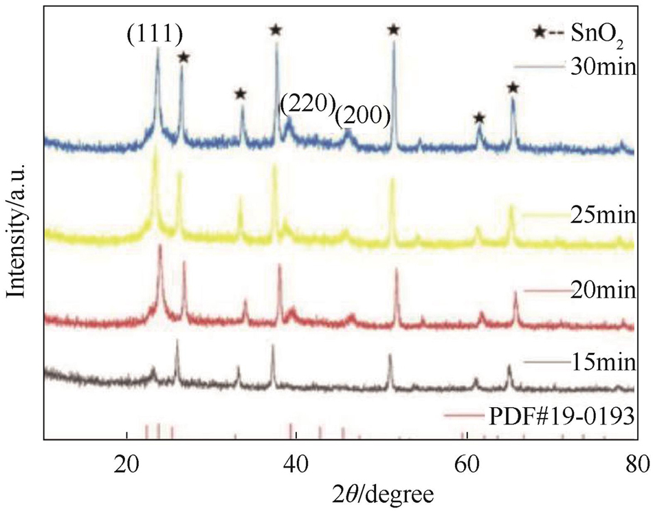
    Fig. 1. Surficial and sectional SEM images of n-type CdTe thin film with deposition time(a)15 min,(b)20 min,(c)25 min,(d)30 min,(e)20 min,(f)30 min.
    XRD patterns of n-typeCdTe thin film with deposition time(a)15 min,(b)20 min,(c)25 min,(d)30 min
    Fig. 2. XRD patterns of n-typeCdTe thin film with deposition time(a)15 min,(b)20 min,(c)25 min,(d)30 min
    Diffuse reflection spectra of n-type CdTe thin film with deposition time(a)UV-Vis diffuse reflection spectra,(b)band-gap spectra
    Fig. 3. Diffuse reflection spectra of n-type CdTe thin film with deposition time(a)UV-Vis diffuse reflection spectra,(b)band-gap spectra
    XPS spectrum of n-type CdTe thin film(a)full spectrum,(b)Cd3d,(c)TeO2,(d)Te3d
    Fig. 4. XPS spectrum of n-type CdTe thin film(a)full spectrum,(b)Cd3d(c)TeO2,(d)Te3d
    PEC properties of n-type CdTe thin film measured in different solution(a)I-V,(b)I-T
    Fig. 5. PEC properties of n-type CdTe thin film measured in different solution(a)I-V,(b)I-T
    PEC properties of n-type CdTe thin film deposited with different time(a)I-V,(b)I-T.
    Fig. 6. PEC properties of n-type CdTe thin film deposited with different time(a)I-V,(b)I-T.
    (a)Schematic diagram of equivalent circuit of electrolytic cell,(b)schematic diagram of simplified equivalent circuit,(c)simple schematic diagram of Nyqusit diagram calculation Ru,Rct,Cd;PEC curves of n-type CdTe thin film deposited with different time(d)Nyquist spectrum,(e)MS spectrum
    Fig. 7. (a)Schematic diagram of equivalent circuit of electrolytic cell,(b)schematic diagram of simplified equivalent circuit,(c)simple schematic diagram of Nyqusit diagram calculation RuRctCd;PEC curves of n-type CdTe thin film deposited with different time(d)Nyquist spectrum,(e)MS spectrum
    PEC properties of n-type CdTe thin film annealed with different temperatures in a vacuum(a)I-V,(b)I-T
    Fig. 8. PEC properties of n-type CdTe thin film annealed with different temperatures in a vacuum(a)I-V,(b)I-T
    PEC properties of n-type CdTe thin film annealed in different conditions(a)I-V,(b)I-T.
    Fig. 9. PEC properties of n-type CdTe thin film annealed in different conditions(a)I-V,(b)I-T.
    EDS mapping of O in n-type CdTe thin film annealed in different conditions(a)annealed in vacuum,(b)CdCl2 coated n-type CdTe annealed in vacuum,(c)annealed in N2 atmosphere
    Fig. 10. EDS mapping of O in n-type CdTe thin film annealed in different conditions(a)annealed in vacuum,(b)CdCl2 coated n-type CdTe annealed in vacuum,(c)annealed in N2 atmosphere
    Deposition time/minThickness/nmCompositional ratios of Cd:TeBandgap/eVPhotocunrent densitiy/μA/cm2Rct

    the flat band

    potential/V

    1511651.06:48.941.5548354.930.357
    2021851.33:48.671.53130376.110.363
    2533851.24:48.761.52148341.550.380
    3055751.51:48.491.51146417.200.377
    Table 1. performance parameters of CdTe thin film with different deposition time
    Annealing conditionVacuum 350℃Vacuum 375℃Vacuum 400℃

    N2

    annealing

    CdCl2

    annealing

    photocurrent densitiy/(μA/cm2158183225152301
    Compositional ratios of Cd:Te49.08:50.9248.47:51.5347.47:52.5345.36:54.6453.55:46.45
    Table 2. PEC properties of different annealing conditions
    Meng CAO, Bin YU, Xiang ZHANG, Cheng-Gang XU, Shan ZHANG, Li-Ying SUN, Xiao-Hong TAN, Yu-Cheng JIANG, Jia-Wei DOU, Lin-Jun WANG. Photoelectrochemical properties of sputtered n-type CdTe thin films[J]. Journal of Infrared and Millimeter Waves, 2022, 41(4): 659
    Download Citation