In this paper, n-type CdTe thin films were prepared by sputtering method. The morphology, structure and optical properties of n-type CdTe thin films deposited with different time and the influence of film thickness and annealing process on the photoelectrochemical (PEC) characteristics of n-type CdTe thin films were studied. The experimental results demonstrated that CdTe thin films with sputtering time of 25 min had better PEC performance. Annealing process could enhance the PEC properties of deposited n-type CdTe thin films. When CdTe thin films were coated with saturated CdCl2 solution and annealed in vacuum at 400 °C, the photocurrents of n-type CdTe thin films achieved 301 μA/cm2.
Fossil resources,such as petroleum,coal and natural gas,are greatly needed in modern society. However,they will be exhausted ultimately with the large-scale exploitation and utilization. Renewable energy,such as solar energy,wind energy and so on,have attracted great attention because of their clean and reusable features. Solar power generation and hydrogen production are important ways of renewable energy utilization. Cadmium telluride(CdTe)has a suitable bandgap(1.5 eV)and high absorption coefficient(104 cm-1)in the visible light range [1-4]. Then,it has been used as an excellent absorption layer in thin film solar cells. As the second lowest-cost material after silicon in the solar cells market,CdTe thin film solar cells have achieved the conversion efficiency of 21.5%[5]. As an absorption layer of photocathode for photo-electro-chemistry(PEC)solar energy water splitting,CdTe photocathode achieved the photocurrent about(24.5 ± 0.5)mA cm-2[6].
However,most of the studies are focused on p-type CdTe for their solar cells and solar energy water splitting applications [7]. Even though n-type CdTe are also investigated[8-10],little studies have been performed on PEC properties of n-type CdTe. During the water splitting process,H+ ions are reduced at the surface of p-type CdTe and O2- ions are oxidized at the surface of n-type CdTe. As known,CdTe can be prepared using various techniques like electrodeposition [11],spray pyrolysis [12],radio frequency sputtering [13-14],close spaced sublimation and vacuum evaporation [15],metal organic chemical vapor deposition [16]. In this paper,PEC properties of n-type CdTe thin films were prepared by sputtering method,which can obtain compact CdTe thin films with good quality.
Then,the PEC properties of n-type CdTe thin films deposited with different time were studied in this paper. And the effect of annealing process on the PEC properties of n-type CdTe thin films was also investigated under illumination of AM 1.5 G,which was contributive to expand their applications on photoelectric devices.
1 Experiments
N-type CdTe thin films were deposited by RF magnetron sputtering method at room temperature and a Cd-rich CdTe compound target(99.999%)was used. Before depositing the n-type CdTe thin films,FTO substrates were ultrasonically cleaned by acetone,ethanol and distilled water for 30 minutes. The cleaned FTO was dried with N2,covered with plastic wrap and placed in the oven for drying. The background pressure before sputtering was less than 8.0×10 -4 Pa. Argon(99.99%)was admitted under control at gas flow rate of 25 sccm(standard cubic centimeter minute)through a needle valve. The sputtering pressure was fixed at 1.2 Pa. CdTe layer was deposited on FTO substrates with the sputtering power of 150 W for 15 ~ 30 min.
The structural properties of n-type CdTe thin films were characterized by X-ray diffraction(XRD,D/MAX2550). Morphologies of n-type CdTe thin films were measured by scanning electron microscopy(SEM,FEI Sirion 200). Compositional ratios were determined by EDS systems attached to the SEM. The optical properties were studied using an ultraviolet-visible spectrophotometer(Jasco UV-570). The valence states of n-type CdTe thin films were determined by X-ray photoelectron spectroscopy(XPS,ESCALAB 250Xi,Thermo SCIENTIFIC). During the XPS measurement,the excitation source was Al Kα and C1s was used as a referencing of the binding energy. The energy of X ray was 1486.6 eV and X-ray tube voltage was15 kV. The size of analyzed area was 500 μm2 and the current was 10 mA. Analysis chamber background vacuum was 2×10⁻⁹ mbar and charges were compensated by electron neutralization gun.
The electrical test and PEC test of CdTe thin film were carried out with three electrode workstation(chi600b). CdTe thin film on FTO was used as the working electrode,Ag/AgCl electrode(1M KCl)was used as the reference electrode and platinum wire(Pt)was used as the counter electrode. The AM 1.5 standard sunlight simulator(Oriel 91159A,100 mW/cm2)was used as light source with spot size of 50 × 50 mm. 0.5 M Na2SO4 solution with pH of 1 ~ 10 was used as the test solution. The I-V curves were measured in the range of -0.8 V(Ag/AgCl)~ 0.8V(Ag/AgCl)with scanning speed of 0.01V/s and scanning time of 400 s. The I-T curves were measured at a constant voltage of 0.6V(Ag / AgCl)with a scanning speed of 0.01v/s. In the process of impedance test,a mixed solution of 0.1 mol/L potassium chloride(KCl),5 mmol/L potassium ferricyanide(K3Fe(CN)6),5 mmol/L potassium ferrocyanide(K4Fe(CN)6)was used as the test solution. The test voltage was -0.4∼0.4 V,the input frequency was 962 Hz and the scanning rate was 0.01 V.
2 Results and discussions
2.1 Physical properties of deposited n-typeCdTe thin films
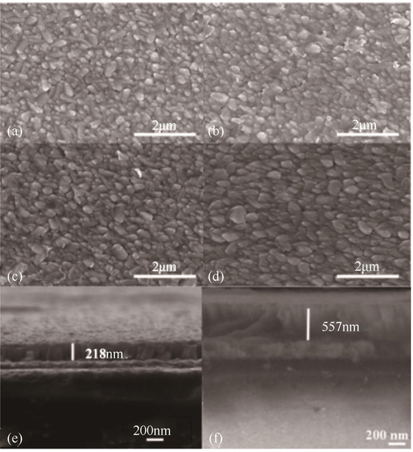
Figure 1 shows the morphologies of n-type CdTe thin films sputtered with time from 15 mins to 30 min. It indicates that the surfaces of CdTe thin films are very compact and the average crystalline sizes are increased slightly with the increasing of deposition time. The cross sectional morphologies also present that compact CdTe thin films have been prepared. As measured from a profilometer,the thicknesses of CdTe thin films are 116,218,338 and 557 nm when the deposition time are 15,20,25 and 30 min,respectively. EDS measurements indicate that the compositional ratios of Cd:Te at deposition time of 15,20,25 and 30 min are 51.06:48.94,51.33:48.67,51.24:48.76,51.51:48.49,respectively. It indicates that Cd rich CdTe thin films have been deposited. Figure 2 presents the structural properties of CdTe thin films analyzed according to XRD patterns. In the XRD patterns,except for the peaks of SnO2 from FTO substrates,the other peaks correspond to CdTe. The diffraction peaks at 2θ=23.7°、39.2°and 45.4° correspond to the(111),(220)and(200)planes of CdTe thin films.
Figure 1.Surficial and sectional SEM images of n-type CdTe thin film with deposition time(a)15 min,(b)20 min,(c)25 min,(d)30 min,(e)20 min,(f)30 min.
Figure 3(a)shows the UV-Vis diffuse reflection spectra of n-type CdTe thin films sputtered with different time. N-type CdTe thin films have obvious absorption in the visible light range from 300 to 800 nm. From the diffuse reflection spectra,the band gaps of CdTe thin films can be calculated according to the Eq. 1:
αhv=K(hv-Eg)1/2 ,
where α is the optical absorption coefficient,hv is the photoelectron energy,Eg is the band gap width,and K is a constant of the material. In Fig. 3(b),the band gaps of n-type CdTe thin films are determined to be 1.55 eV,1.53eV,1.52eV,1.51eV,respectively. Figure 4 presents the XPS spectra of n-type CdTe thin films. It can be seen that Cd and Te exist in the films. The binding energies at 582.7 and 572.2 eV correspond to Te2-3d3/2 and Te2-3d5/2[18]. The width between Te2-3d3/2 and Te2-3d5/2 is 10 eV,which indicates that Te exists as Te2- in n-type CdTe films. The peaks at 575.18 eV and 585.52 eV show that TeO2 exist in CdTe thin films. The peaks at 411.7 eV and 405.0 eV correspond to Cd3d3/2 and Cd3d5/2. The width between Cd3d3/2 and Cd3d5/2 is 6.7 eV,which indicates that Cd2+ is existed in n-type CdTe films [19].
Figure 3.Diffuse reflection spectra of n-type CdTe thin film with deposition time(a)UV-Vis diffuse reflection spectra,(b)band-gap spectra
2.2 Photoelectrochemical properties of n-type CdTe thin films
The conductive type of the film can be judged by linear scanning the volt-current characteristic curves,and the light-dark curves of the films under different voltages can be obtained by continuously cutting the light under AM1.5 light. In Fig. 5(a),the IV curves of CdTe thin films were measured from -0.8 V to 0.8V under acidic,alkaline and neutral conditions. It can be seen from Fig. 5(a)that the photocurrent density is larger when the sample is forward biased,which indicates that the conductivity type of the CdTe thin films is n-type. Figure 5(b)presents the I-T curves of CdTe thin films. A constant voltage of 0.6 V(Ag/AgCl)is applied during the measurement,and the scanning speed is 0.01 V/S. From the I-T curves,it can be calculated that the average photocurrent densities of CdTe thin films under acidic(pH=1),alkaline(pH=10),and neutral(pH=7)conditions are 60,148,and 25 μA/cm2. It can be seen that different test environments have a great effect on the photocurrent values of the CdTe thin films. The photocurrent in acidic conditions is relatively unstable,which may be due to the dissolution of the CdTe thin films in the acidic environment and then causes the damage of the CdTe thin films. By comprehensively comparing the I-V and I-T data graphs in the three pH environments,it indicates
Figure 5.PEC properties of n-type CdTe thin film measured in different solution(a)I-V,(b)I-T
that the alkaline environment is a more suitable measurement environment. It is because of that an oxygen evolving photoanode material must be an n-type semiconductor,such that the electric field generated by band bending drives holes toward the surface. Due to a potential drop across the Helmholtz layer,the positions of the Fermi level of semiconductors shift up by the adsorption of excess H+/OH- species [20]. Then,the reducing power of electrons(i.e.,a more negative electrode potential)will be increased by increasing the solution pH. Therefore,the rate of photocatalytic reaction increases at higher pH values. Then,the alkaline environment is selected to measure the PEC properties of n-type CdTe thin films.
Figure 6(a)is the I-V curves of CdTe thin films deposited with different sputtering time in alkaline environment,which also confirms that n-type CdTe thin films have been achieved. From the I-T curves in Fig. 6(b),it can be calculated that the average photocurrent densities enlarge from 48 μA/cm2,130 μA/cm2,148 μA/cm2 to 146 μA/cm2 with the increasing of deposition time from 15 to 30 min. Under the same bias voltage,the photocurrent densities of CdTe films are first increased and then decreased with the increasing of film thickness. When the thicknesses of CdTe films are small,the corrosion of electrolyte solutions will damage the surface of CdTe films rapidly,which will lead to a significant change of the surface morphology and composition of CdTe films. But it does not contribute to the transportation and separation of photogenerated carriers,if the thickness of CdTe films is too large. In these experiments,the photocurrents of the films with the deposition time of 25 min and 30 min are relatively stable without significant attenuation. The photocurrent curves of the films with deposition time of 15 min and 20 min show a decay trend,which may be due to the severe corrosion of the thinner thickness of n-type CdTe thin films. From Fig. 6,it can be concluded that the optimal sputtering time is 25 min. Using the open circuit voltage as the input voltage,the electrochemical impedance spectroscopies of the films were tested in the same solution,and the electrochemical polarization complex plane diagrams(Nyquist diagram)were presented,as shown in Fig. 7. The electrical properties can be calculated from the diagram in Fig. 7(a). The characteristic parameters Rct,Ru,Cd and σ are determined,it can be seen that the solution ohmic resistance Ru of the CdTe thin films with different sputtering time basically does not change,all being around 37.5 Ω,while the data of the charge transfer resistance Rct of the samples have obvious changes. The Rct values of CdTe thin films deposited at sputtered duration of 15,20,25 and 30 min are 354.93 Ω,376.11 Ω,341.55Ω,and 417.20 Ω,respectively. Among them,the Rct value of the sample with a sputtering time of 25 min is the smallest,which is 341.55 Ω. The smaller Rct values,the better of PEC properties of CdTe thin films. the Compared with other samples,the sample with a sputtering time of 25 min has better film electrical properties. In order to further understand the electrical properties of the products,Mott-Schottky test was performed on CdTe films with different thicknesses. The test voltage is -0.4 to 0 V,and the input frequency is 962 Hz. The intersection of the tangent of the curve and the X axis is the flat-band potential. The flat-band potential of a semiconductor is an important factor in explaining the charge transfer process across the semiconductor-electrolyte junction of the cell. It can be seen from Fig. 7(b)that the slopes of the curves are all positive,which indicates that the conductivity types of the films are all n-type. The flat band voltages of the samples with different sputtering time are 0.357 V,0.363V,0.380 V and 0.377 V,respectively. The change of flat band potential may be due to the surface states presented on CdTe films. And higher flat band potential is contributive to improve the photocatalytic properties of CdTe films. Based on Fig. 7,it can be seen that the sample with a sputtering time of 25mins has better film electrical properties than other samples. It indicates that 25 min is a relatively suitable sputtering time for n-type CdTe thin films. The performance parameters of CdTe thin film with different deposition time have been summarized in Table 1.
Figure 6.PEC properties of n-type CdTe thin film deposited with different time(a)I-V,(b)I-T.
Figure 7.(a)Schematic diagram of equivalent circuit of electrolytic cell,(b)schematic diagram of simplified equivalent circuit,(c)simple schematic diagram of Nyqusit diagram calculation Ru,Rct,Cd;PEC curves of n-type CdTe thin film deposited with different time(d)Nyquist spectrum,(e)MS spectrum
N-type CdTe thin films with deposition time of 25 min were annealed under different temperatures in vacuum. Figure 8(a)shows the I-V curves of annealed n-type CdTe thin films,which were measured in an alkaline environment(pH=10). After annealing process,CdTe thin films are still n-type. Figure 8(b)shows the I-T curves of CdTe thin films annealed with different temperatures in vacuum. It can be seen from the Fig. 8(b)that the photocurrent densities are 158 μA/cm2,
Figure 8.PEC properties of n-type CdTe thin film annealed with different temperatures in a vacuum(a)I-V,(b)I-T
183 μA/cm2,225 μA/cm2 at the annealing temperatures of 350 ℃,375 ℃ and 400 ℃. When the annealing temperature exceeds 400 ℃,CdTe thin films will disappear from the FTO substrates due to the evaporation of the relative thin CdTe films. With the increasing of annealing temperature from 350 ℃ to 400 ℃,EDS measurements indicate that the compositional ratios of Cd:Te in CdTe thin films are 49.08:50.92,48.47:51.53,47.47:52.53,respectively. The annealing process will lead to the evaporation loss of Cd in CdTe thin films. As previously discussed in Sect. 3.1,Cd has higher atomic composition than Te regardless of the thin film thickness used in this work. It has been reported by researchers that Cd-rich CdTe thin films are n-type while Te-rich CdTe thin films are p-type [21]. However,despite the loss of Cd after annealing process,which makes the atomic composition of Te to be higher than Cd in CdTe thin films,the materials still remain n-type as seen in Fig. 8(a). This therefore shows that EDS technique may not be a suitable technique to qualitatively ascertain the electrical conductivity type of semiconductors. Figure 9(a)shows the I-V curves of CdTe thin films annealed in nitrogen atmosphere at 400 ℃. CdTe thin films are still n-type at this condition. I-T curves in Fig. 9(b)indicate that the average photocurrent density of the sample is calculated to be 152 μA/cm2. Even though the photocurrent value is obviously larger than that of the as-deposited samples,it is smaller than that of n-type CdTe thin films annealed in vacuum. Besides,the photocurrent is decayed obviously after annealed in nitrogen atmosphere. EDS measurements indicate that the compositional ratio of Cd:Te is 45.36:54.64 when CdTe thin film is annealed in nitrogen atmosphere. It indicates that the element Cd in CdTe thin films will evaporate during the annealing process,which leads to the decreasing of the photocurrents of CdTe thin films [22]. Annealing in nitrogen atmosphere will cause more loss of Cd element than in vaccum. Then,saturated
Figure 9.PEC properties of n-type CdTe thin film annealed in different conditions(a)I-V,(b)I-T.
CdCl2 solution was applied onto the surface of CdTe thin films and then annealed in vacuum at 400 ℃. Figure 9(b)indicates that the photocurrent of annealed CdTe thin films after applying saturated CdCl2 condition is greatly enhanced,which reaches 301 μA/cm2. EDS measurements indicate that the compositional ratio of Cd:Te is 53.55:46.45. Then,it can be concluded that,the compositional ratio of Cd element in CdTe thin films has a great influence on the photocurrent values and their stabilities,as shown in Table 2. But the conductive types of CdTe thin films are not changed by the compositional ratio of Cd element. Cd-rich CdTe thin films have better PEC properties,which can be achieved by applying saturated CdCl2 solution onto the surface of CdTe thin films and annealed in vacuum. Besides the element of Cd,the influence of O element at the surface of the sample was also investigated. The EDS mappings of O were presented in Fig. 10. It can be seen that the distribution of O element on the surface of CdTe film turns denser when CdTe thin films were annealed in N2 atmosphere. The elemental compositional ratio of O:Cd:Te in CdTe thin films annealed in vacuum, CdCl2 coated CdTe thin films annealed in vacuum,and CdTe thin films annealed in N2 atmosphere are 20.15:38.9:38.31;20.05:42.28:37.67;and 23.05:39.74,:37.22,respectively. CdTe thin films annealed in N2 atmosphere have more O content at the sample surface,which may be due to the fact that some O are mixed into the N2 atmosphere,even though high pure nitrogen(99.99%)is used in the annealing process. From the EDS mapping,we really find that O element is segregated to grain boundaries at the surface of CdTe thin films. The existence of O at the surface of CdTe thin films will also decrease the PEC properties of CdTe thin films. Beside these,the other studies have reported the surface modification of CdTe thin films,such as fabrication of CdTe/CdS PN junction. The presence of this junction should improve the charge separation and the deep valence band maximum of CdS also enhances charge separation by suppressing the diffusion of holes to the photocathode surface [23]. Deposition of TiO2 and Pt can also enhance the photocurrents and stabilities of CdTe thin films [24-25]. For n-type CdTe,deposition of p-type window layer,such as CdS:Cu,is also worthy of studies in detail. The PN junction of p-type CdS:Cu/n-type CdTe can also enhance the PEC properties of n-type CdTe thin films [26].
Annealing condition
Vacuum 350℃
Vacuum 375℃
Vacuum 400℃
N2
annealing
CdCl2
annealing
photocurrent densitiy/(μA/cm2)
158
183
225
152
301
Compositional ratios of Cd:Te
49.08:50.92
48.47:51.53
47.47:52.53
45.36:54.64
53.55:46.45
Table 2. PEC properties of different annealing conditions
Figure 10.EDS mapping of O in n-type CdTe thin film annealed in different conditions(a)annealed in vacuum,(b)CdCl2 coated n-type CdTe annealed in vacuum,(c)annealed in N2 atmosphere
N-type CdTe thin films have been fabricated by sputtering method and its PEC properties were studied. CdTe thin films have better PEC properties under alkaline electrolyte solution,which confirms its n-type properties. The thickness of sputtered CdTe thin films increased from116 nm to 557 nm when the deposition time is increased from 15 to 30 min. The photocurrents of n-type CdTe thin films can reach 148 μA/cm2 when the sputtering time is 25min. The photocurrent densities are 158 μA/cm2,183 μA/cm2,225 μA/cm2 when the annealing temperatures are 350 ℃,375 ℃ and 400 ℃ in vacuum,respectively. When n-type CdTe thin films were coated with saturated CdCl2 solution and annealed in vacuum at 400 ℃,its photocurrents can be enhanced to 301 μA/cm2.The PEC properties of n-type CdTe thin films can be further improved by fabrication of suitable PN junctions,which still needs further studies.