[1] K S Novoselov. Electric field effect in atomically thin carbon films. Science, 306, 666(2004).
[2] B J Feng, J Zhang, Q Zhong et al. Experimental realization of two-dimensional boron sheets. Nat Chem, 8, 563(2016).
[3] C Kamal, A Chakrabarti, M Ezawa. Aluminene as highly hole-doped graphene. New J Phys, 17, 083014(2015).
[4] M L Tao, Y B Tu, K Sun et al. Gallenene epitaxially grown on Si(111). 2D Mater, 5, 035009(2018).
[5] D Singh, S K Gupta, I Lukačević et al. Indiene 2D monolayer: A new nanoelectronic material. RSC Adv, 6, 8006(2016).
[6] P Vogt, P de Padova, C Quaresima et al. Silicene: compelling experimental evidence for graphenelike two-dimensional silicon. Phys Rev Lett, 108, 155501(2012).
[7] E Bianco, S Butler, S S Jiang et al. Stability and exfoliation of germanane: A germanium graphane analogue. ACS Nano, 7, 4414(2013).
[8] F F Zhu, W J Chen, Y Xu et al. Epitaxial growth of two-dimensional stanene. Nat Mater, 14, 1020(2015).
[9] J Yuhara, B J He, N Matsunami et al. Graphene's latest cousin: Plumbene epitaxial growth on a “nano WaterCube”. Adv Mater, 31, 1901017(2019).
[10] L K Li, Y J Yu, G J Ye et al. Black phosphorus field-effect transistors. Nat Nanotechnol, 9, 372(2014).
[11] S L Zhang, Z Yan, Y F Li et al. Atomically thin arsenene and antimonene: Semimetal-semiconductor and indirect-direct band-gap transitions. Angew Chem Int Ed, 54, 3112(2015).
[12] J P Ji, X F Song, J Z Liu et al. Two-dimensional antimonene single crystals grown by van der Waals epitaxy. Nat Commun, 7, 13352(2016).
[13] F Reis, G Li, L Dudy et al. Bismuthene on a SiC substrate: A candidate for a high-temperature quantum spin Hall material. Science, 357, 287(2017).
[14] Z L Zhu, X L Cai, S Yi et al. Multivalency-driven formation of Te-based monolayer materials: A combined first-principles and experimental study. Phys Rev Lett, 119, 106101(2017).
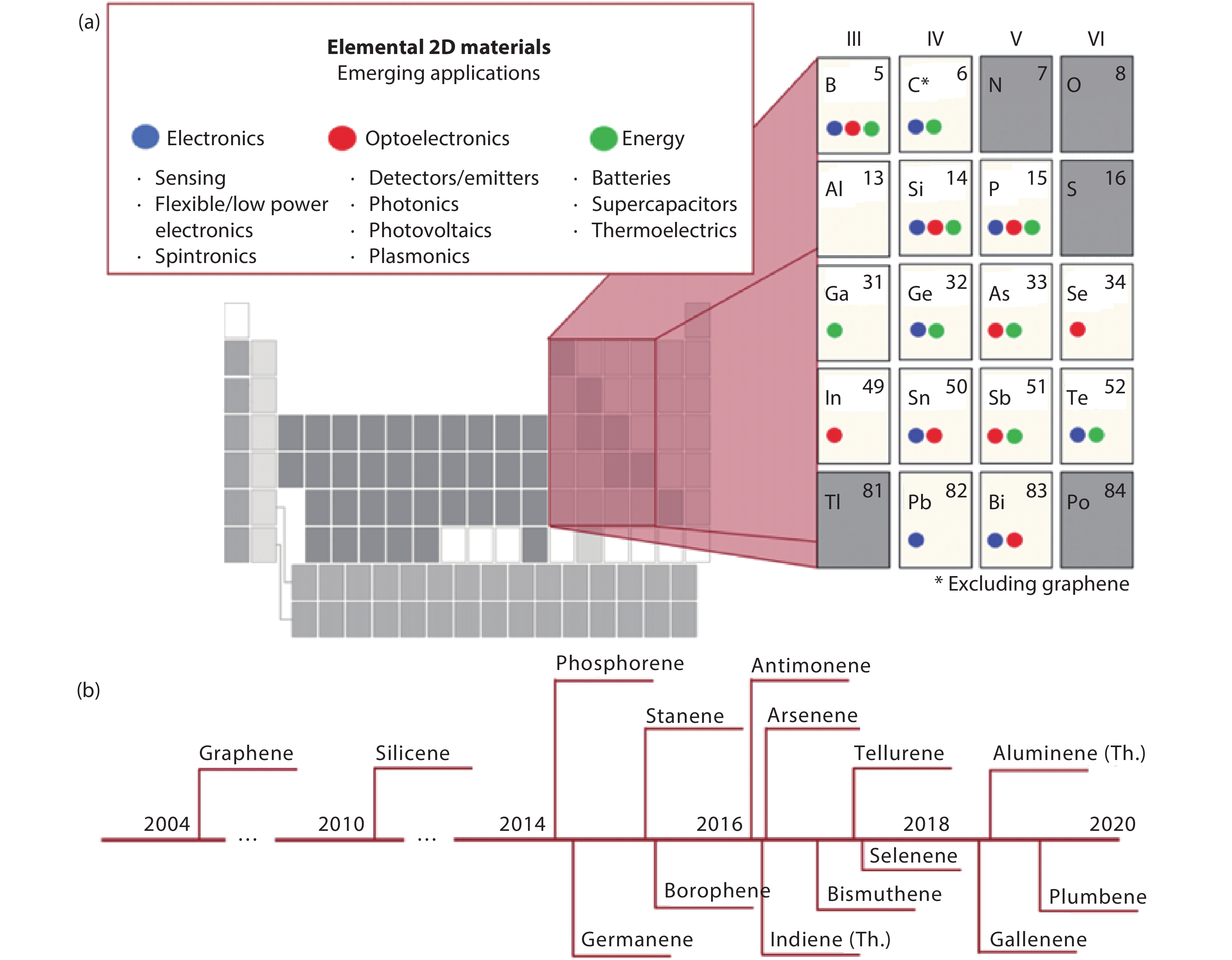
[15] N R Glavin, R Rao, V Varshney et al. Emerging applications of elemental 2D materials. Adv Mater, 32, 1904302(2020).
[16] J S Qiao, Y H Pan, F Yang et al. Few-layer tellurium: One-dimensional-like layered elementary semiconductor with striking physical properties. Sci Bull, 63, 159(2018).
[17] S Q Deng, J Koehler, A Simon. Unusual lone pairs in tellurium and their relevance for superconductivity. Angew Chem Int Ed, 45, 599(2006).
[18] A Coker, T Lee, T P Das. Investigation of the electronic properties of tellurium: Energy-band structure. Phys Rev B, 22, 2968(1980).
[19] M Hulin. Electron band structure of tellurium. J Phys Chem Solids, 27, 441(1966).
[20] R E Beissner. Electron energy bands in tellurium. Phys Rev, 145, 479(1966).
[21] H G Junginger. Electronic band structure of tellurium. Solid State Commun, 5, 509(1967).
[22] M H Weiler. Landau levels in the valence band of tellurium. Solid State Commun, 8, 1017(1970).
[23] D Thanh. Effective mass approximation for acceptors in tellurium. Solid State Commun, 9, 631(1971).
[24] H Shinno, R Yoshizaki, S Tanaka et al. Conduction band structure of tellurium. J Phys Soc Jpn, 35, 525(1973).
[25] R Enderlein, A Hache. Valence and conduction band structure and infrared optical properties of tellurium in the presence of pressure. Phys Status Solidi B, 60, 739(1973).
[26] L A Agapito, N Kioussis, W A Goddard et al. Novel family of chiral-based topological insulators: Elemental tellurium under strain. Phys Rev Lett, 110, 176401(2013).
[27] S Q Lin, W Li, Z W Chen et al. Tellurium as a high-performance elemental thermoelectric. Nat Commun, 7, 10287(2016).
[28] Y Akahama, N Okawa, T Sugimoto et al. Coexistence of a metastable double hcp phase in bcc–fcc structure transition of Te under high pressure. Jpn J Appl Phys, 57, 025601(2018).
[29] Y Tanaka, S P Collins, S W Lovesey et al. Determination of the absolute chirality of tellurium using resonant diffraction with circularly polarized X-rays. J Phys Condens Matter, 22, 122201(2010).
[30] M Hirayama, R Okugawa, S Ishibashi et al. Weyl node and spin texture in trigonal tellurium and selenium. Phys Rev Lett, 114, 206401(2015).
[31] K Nakayama, M Kuno, K Yamauchi et al. Band splitting and Weyl nodes in trigonal tellurium studied by angle-resolved photoemission spectroscopy and density functional theory. Phys Rev B, 95, 125204(2017).
[32] M Sakano, M Hirayama, T Takahashi et al. Radial spin texture in elemental tellurium with chiral crystal structure. Phys Rev Lett, 124, 136404(2020).
[33] Z Y Dong, Y H Ma. Atomic-level handedness determination of chiral crystals using aberration-corrected scanning transmission electron microscopy. Nat Commun, 11, 1588(2020).
[34]
[35] S S Kabalkina, L F Vereshchagin, B M Shulenin. Phase transitions in tellurium at high pressures. J Exp Theor Phys, 45, 2073(1964).
[36] J C Jamieson, D B McWhan. Crystal structure of tellurium at high pressures. J Chem Phys, 43, 1149(1965).
[37] K Aoki, O Shimomura, S Minomura. Crystal structure of the high-pressure phase of tellurium. J Phys Soc Jpn, 48, 551(1980).
[38] Y Akahama, M Kobayashi, H Kawamura. Pressure-induced superconductivity and phase transition in selenium and tellurium. Solid State Commun, 84, 803(1992).
[39] Y C Wang, J Lv, L Zhu et al. Crystal structure prediction via particle-swarm optimization. Phys Rev B, 82, 094116(2010).
[40] E J Reed. Two-dimensional tellurium. Nature, 552, 40(2017).
[41]
[42] D Liu, X Q Lin, D Tománek. Microscopic mechanism of the helix-to-layer transformation in elemental group VI solids. Nano Lett, 18, 4908(2018).
[43] L D Xian, Paz A Pérez, E Bianco et al. Square selenene and tellurene: Novel group VI elemental 2D materials with nontrivial topological properties. 2D Mater, 4, 041003(2017).
[44] W Zhang, Q S Wu, O V Yazyev et al. Topological phase transitions driven by strain in monolayer tellurium. Phys Rev B, 98, 115411(2018).
[45] T Paulauskas, F G Sen, C Sun et al. Stabilization of a monolayer tellurene phase at CdTe interfaces. Nanoscale, 11, 14698(2019).
[46] L J Qi, J Han, W Gao et al. Monolayer tellurenyne assembled with helical telluryne: Structure and transport properties. Nanoscale, 11, 4053(2019).
[47] Y Wang, C C Xiao, M G Chen et al. Two-dimensional ferroelectricity and switchable spin-textures in ultra-thin elemental Te multilayers. Mater Horiz, 5, 521(2018).
[48] C Wang, X Y Zhou, J S Qiao et al. Charge-governed phase manipulation of few-layer tellurium. Nanoscale, 10, 22263(2018).
[49] Y Xiang, S J Gao, R G Xu et al. Phase transition in two-dimensional tellurene under mechanical strain modulation. Nano Energy, 58, 202(2019).
[50] B Z Wu, X H Liu, J R Yin et al. Bulk
[51] Y J Zhu, X L Hu, W W Wang. Poly(vinylpyrrolidone): a new reductant for preparation of tellurium nanorods, nanowires, and tubes from TeO2. Nanotechnology, 17, 645(2006).
[52] H S Qian, S H Yu, J Y Gong et al. High-quality luminescent tellurium nanowires of several nanometers in diameter and high aspect ratio synthesized by a poly (vinyl pyrrolidone)-assisted hydrothermal process. Langmuir, 22, 3830(2006).
[53] M Mo, J Zeng, X Liu et al. Controlled hydrothermal synthesis of thin single-crystal tellurium nanobelts and nanotubes. Adv Mater, 14, 1658(2002).
[54] Q S Wang, M Safdar, K Xu et al. Van der Waals epitaxy and photoresponse of hexagonal tellurium nanoplates on flexible mica sheets. ACS Nano, 8, 7497(2014).
[55] W Z Wu, G Qiu, Y X Wang et al. Tellurene: its physical properties, scalable nanomanufacturing, and device applications. Chem Soc Rev, 47, 7203(2018).
[56] H O H Churchill, G J Salamo, S Q Yu et al. Toward single atom chains with exfoliated tellurium. Nanoscale Res Lett, 12, 1(2017).
[57] Y Lin, Y Wu, R Wang et al. Two-dimensional tellurium nanosheets for photoacoustic imaging-guided photodynamic therapy. Chem Commun, 54, 8579(2018).
[58] Z J Xie, C Y Xing, W C Huang et al. Ultrathin 2D nonlayered tellurium nanosheets: Facile liquid-phase exfoliation, characterization, and photoresponse with high performance and enhanced stability. Adv Funct Mater, 28, 1705833(2018).
[59] F Zhang, G W Liu, Z P Wang et al. Broadband nonlinear absorption properties of two-dimensional hexagonal tellurene nanosheets. Nanoscale, 11, 17058(2019).
[60] J Guo, J L Zhao, D Z Huang et al. Two-dimensional tellurium-polymer membrane for ultrafast photonics. Nanoscale, 11, 6235(2019).
[61] Y Wang, G Qiu, R Wang et al. Field-effect transistors made from solution-grown two-dimensional tellurene. Nat Electron, 1, 228(2018).
[62] Y X Wang, R de Souza Borges Ferreira, R X Wang et al. Data-driven and probabilistic learning of the process-structure-property relationship in solution-grown tellurene for optimized nanomanufacturing of high-performance nanoelectronics. Nano Energy, 57, 480(2019).
[63] Y S Chen, J Ding, X M He et al. Synthesis of tellurium nanosheet for use in matrix assisted laser desorption/ionization time-of-flight mass spectrometry of small molecules. Microchim Acta, 185, 1(2018).
[64] M Gao, X W Wang, Y Z Hong et al. One-pot hydrothermal synthesis of thin tellurene nanosheet and its formation mechanism. J Nanomater, 2019, 1(2019).
[65] X C Huang, J Q Guan, Z J Lin et al. Epitaxial growth and band structure of Te film on graphene. Nano Lett, 17, 4619(2017).
[66] J L Chen, Y W Dai, Y Q Ma et al. Ultrathin
[67] S Khatun, A Banerjee, A J Pal. Nonlayered tellurene as an elemental 2D topological insulator: Experimental evidence from scanning tunneling spectroscopy. Nanoscale, 11, 3591(2019).
[68] S Yang, B Chen, Y Qin et al. Highly crystalline synthesis of tellurene sheets on two-dimensional surfaces: Control over helical chain direction of tellurene. Phys Rev Mater, 2, 104002(2018).
[69] A Apte, E Bianco, A Krishnamoorthy et al. Polytypism in ultrathin tellurium. 2D Mater, 6, 015013(2018).
[70] J Peng, Y Pan, Z Yu et al. Two-dimensional tellurium nanosheets exhibiting an anomalous switchable photoresponse with thickness dependence. Angew Chem Int Ed, 57, 13533(2018).
[71] Y L Dong, B W Zeng, X J Zhang et al. Study on the strain-induced mechanical property modulations in monolayer Tellurene. J Appl Phys, 125, 064304(2019).
[72] Z B Gao, F Tao, J Ren. Unusually low thermal conductivity of atomically thin 2D tellurium. Nanoscale, 10, 12997(2018).
[73] S Sharma, N Singh, U Schwingenschlögl. Two-dimensional tellurene as excellent thermoelectric material. ACS Appl Energy Mater, 1, 1950(2018).
[74] G Liu, Z B Gao, J Ren. Anisotropic thermal expansion and thermodynamic properties of monolayer
[75] G Qiu, S Y Huang, M Segovia et al. Thermoelectric performance of 2D tellurium with accumulation contacts. Nano Lett, 19, 1955(2019).
[76] C S Lin, W D Cheng, G L Chai et al. Thermoelectric properties of two-dimensional selenene and tellurene from group-VI elements. Phys Chem Chem Phys, 20, 24250(2018).
[77] K Chang, J W Liu, H C Lin et al. Discovery of robust in-plane ferroelectricity in atomic-thick SnTe. Science, 353, 274(2016).
[78]
[79] X R Cai, Y Y Ren, M H Wu et al. Strain-induced phase transition and giant piezoelectricity in monolayer tellurene. Nanoscale, 12, 167(2020).
[80] Y Y Liu, W Z Wu, W A III Goddard. Tellurium: fast electrical and atomic transport along the weak interaction direction. J Am Chem Soc, 140, 550(2018).
[81] J H Yan, H Pang, L Xu et al. Excellent device performance of sub-5-nm monolayer tellurene transistors. Adv Electron Mater, 5, 1900226(2019).
[82] G Qiu, Y Wang, Y Nie et al. Quantum transport and band structure evolution under high magnetic field in few-layer tellurene. Nano Lett, 18, 5760(2018).
[83] X L Ren, Y Wang, Z T Xie et al. Gate-tuned insulator–metal transition in electrolyte-gated transistors based on tellurene. Nano Lett, 19, 4738(2019).
[84] P K Li, J D Sau, I Appelbaum. Robust zero-energy bound states in a helical lattice. Phys Rev B, 96, 115446(2017).
[85] P K Li, I Appelbaum. Intrinsic two-dimensional states on the pristine surface of tellurium. Phys Rev B, 97, 201402(2018).
[86]
[87] C Niu, G Qiu, Y X Wang et al. Gate-tunable strong spin-orbit interaction in two-dimensional tellurium probed by weak antilocalization. Phys Rev B, 101, 205414(2020).
[88] Y Y Pan, S Y Gao, L Yang et al. Dependence of excited-state properties of tellurium on dimensionality: From bulk to two dimensions to one dimensions. Phys Rev B, 98, 085135(2018).
[89] S Deckoff-Jones, Y X Wang, H T Lin et al. Tellurene: A multifunctional material for midinfrared optoelectronics. ACS Photonics, 6, 1632(2019).
[90] Q L Bao, H Zhang, Y Wang et al. Atomic-layer graphene as a saturable absorber for ultrafast pulsed lasers. Adv Funct Mater, 19, 3077(2009).
[91] J Du, Q K Wang, G B Jiang et al. Ytterbium-doped fiber laser passively mode locked by few-layer molybdenum disulfide (MoS2) saturable absorber functioned with evanescent field interaction. Sci Rep, 4, 6346(6346).
[92] Z Q Luo, Y Z Huang, J Weng et al. 1.06
[93] S F Zhang, X Y Zhang, H Wang et al. Size-dependent saturable absorption and mode-locking of dispersed black phosphorus nanosheets. Opt Mater Express, 6, 3159(2016).
[94] L M Wu, W C Huang, Y Z Wang et al. 2D tellurium based high-performance all-optical nonlinear photonic devices. Adv Funct Mater, 29, 1806346(2019).
[95] W F Zhang, G M Wang, F Xing et al. Passively Q-switched and mode-locked erbium-doped fiber lasers based on tellurene nanosheets as saturable absorber. Opt Express, 28, 14729(2020).
[96] M Amani, C L Tan, G Zhang et al. Solution-synthesized high-mobility tellurium nanoflakes for short-wave infrared photodetectors. ACS Nano, 12, 7253(2018).
[97] C F Shen, Y H Liu, J B Wu et al. Tellurene photodetector with high gain and wide bandwidth. ACS Nano, 14, 303(2020).
[98] S Y Gao, C Q Sun, X Zhang. Ultra-strong anisotropic photo-responsivity of bilayer tellurene: A quantum transport and time-domain first principle study. Nanophotonics, 9, 1931(2019).
[99] S Berweger, G Qiu, Y X Wang et al. Imaging carrier inhomogeneities in ambipolar tellurene field effect transistors. Nano Lett, 19, 1289(2019).
[100] J J Wang, Y R Guo, H Shen et al. A first-principles study of strain tuned optical properties in monolayer tellurium. RSC Adv, 9, 41703(2019).
[101] H H Ma, W Hu, J L Yang. Control of highly anisotropic electrical conductance of tellurene by strain-engineering. Nanoscale, 11, 21775(2019).
[102] Y C Du, G Qiu, Y X Wang et al. One-dimensional van der waals material tellurium: Raman spectroscopy under strain and magneto-transport. Nano Lett, 17, 3965(2017).
[103] X H Wang, D W Wang, A J Yang et al. Effects of adatom and gas molecule adsorption on the physical properties of tellurene: A first principles investigation. Phys Chem Chem Phys, 20, 4058(2018).
[104] W P Xu, L Y Gan, R Wang et al. Surface adsorption and vacancy in tuning the properties of tellurene. ACS Appl Mater Interfaces, 12, 19110(2020).
[105] D W Wang, A J Yang, T S Lan et al. Tellurene based chemical sensor. J Mater Chem A, 7, 26326(2019).
[106] D Wines, J A Kropp, G Chaney et al. Electronic properties of bare and functionalized two-dimensional (2D) tellurene structures. Phys Chem Chem Phys, 22, 6727(2020).
[107] D K Liu, Y G Gui, C Ji et al. Adsorption of SF6 decomposition components over Pd (111): A density functional theory study. Appl Surf Sci, 465, 172(2019).
[108] H P Cui, K Zheng, L Q Tao et al. Monolayer tellurene-based gas sensor to detect SF6 decompositions: A first-principles study. IEEE Electron Device Lett, 40, 1522(2019).
[109] Z F Liang, Y Wang, C Q Hua et al. Electronic structures of ultra-thin tellurium nanoribbons. Nanoscale, 11, 14134(2019).
[110] Y Lv, Y Liu, W J Qin et al. Prediction of stable and high-performance charge transport in zigzag tellurene nanoribbons. IEEE Trans Electron Devices, 66, 2365(2019).
[111] H Li, K Wu, S J Yang et al. Anomalous phase transition behavior in hydrothermal grown layered tellurene. Nanoscale, 11, 20245(2019).
[112] S J Gao, Y X Wang, R X Wang et al. Piezotronic effect in 1D van der Waals solid of elemental tellurium nanobelt for smart adaptive electronics. Semicond Sci Technol, 32, 104004(2017).
[113] J Kang, S Tongay, J Zhou et al. Band offsets and heterostructures of two-dimensional semiconductors. Appl Phys Lett, 102, 012111(2013).
[114] J M Liao, B S Sa, J Zhou et al. Design of high-efficiency visible-light photocatalysts for water splitting: MoS2/AlN(GaN) heterostructures. J Phys Chem C, 118, 17594(2014).
[115] Q K Wu, S K Jang, S Park et al.
[116] X R Zhang, Z S Meng, D W Rao et al. Efficient band structure tuning, charge separation, and visible-light response in ZrS2-based van der Waals heterostructures. Energy Environ Sci, 9, 841(2016).
[117] C Si, Z Z Lin, J Zhou et al. Controllable Schottky barrier in GaSe/graphene heterostructure: The role of interface dipole. 2D Mater, 4, 015027(2016).
[118] K Wu, H H Ma, Y Z Gao et al. Highly-efficient heterojunction solar cells based on two-dimensional tellurene and transition metal dichalcogenides. J Mater Chem A, 7, 7430(2019).
[119] X L Cai, X T Jia, Y J Liu et al. Enhanced carrier mobility and tunable electronic properties in α-tellurene monolayer via an α-tellurene and h-BN heterostructure. Phys Chem Chem Phys, 22, 6434(2020).
[120] X M Qin, W Hu, J L Yang. Tunable Schottky and Ohmic contacts in graphene and tellurene van der Waals heterostructures. Phys Chem Chem Phys, 21, 23611(2019).
[121] J H Yan, X Y Zhang, Y Y Pan et al. Monolayer tellurene–metal contacts. J Mater Chem C, 6, 6153(2018).
[122] H Pang, J H Yan, J Yang et al. Bilayer tellurene–metal interfaces. J Semicond, 40, 062003(2019).
[123] W L Zhang, D H Chang, Q Gao et al. Interlayer coupling and external electric field tunable electronic properties of a 2D type-I α-tellurene/MoS2 heterostructure. J Mater Chem C, 6, 10256(2018).
[124] Z Ma, Y S Wang, Y T Wei et al. A type-II C2N/α-Te van der Waals heterojunction with improved optical properties by external perturbation. Phys Chem Chem Phys, 21, 21753(2019).
[125] M M Obeid. Tuning the electronic and optical properties of type-I PbI2/α-tellurene van der Waals heterostructure via biaxial strain and external electric field. Appl Surf Sci, 508, 144824(2020).
[126] W Y Yu, S F Li, X L Cai et al. Ferromagnetic half-metal properties of two dimensional vertical tellurene/VS2 heterostructure: A first-principles study. Comput Mater Sci, 171, 109215(2020).
[127] H L Zhuang, R G Hennig. Stability and magnetism of strongly correlated single-layerVS2. Phys Rev B, 93, 054429(2016).
[128] H R Fuh, C R Chang, Y K Wang et al. Newtype single-layer magnetic semiconductor in transition-metal dichalcogenides VX2 (X = S, Se and Te). Sci Rep, 6, 32625(2016).