
Xiaolin Cai, Xiaoyu Han, Chunxiang Zhao, Chunyao Niu, Yu Jia. Tellurene: An elemental 2D monolayer material beyond its bulk phases without van der Waals layered structures[J]. Journal of Semiconductors, 2020, 41(8): 081002
- Journal of Semiconductors
- Vol. 41, Issue 8, 081002 (2020)
Abstract
1. Overview of elemental two-dimensional materials
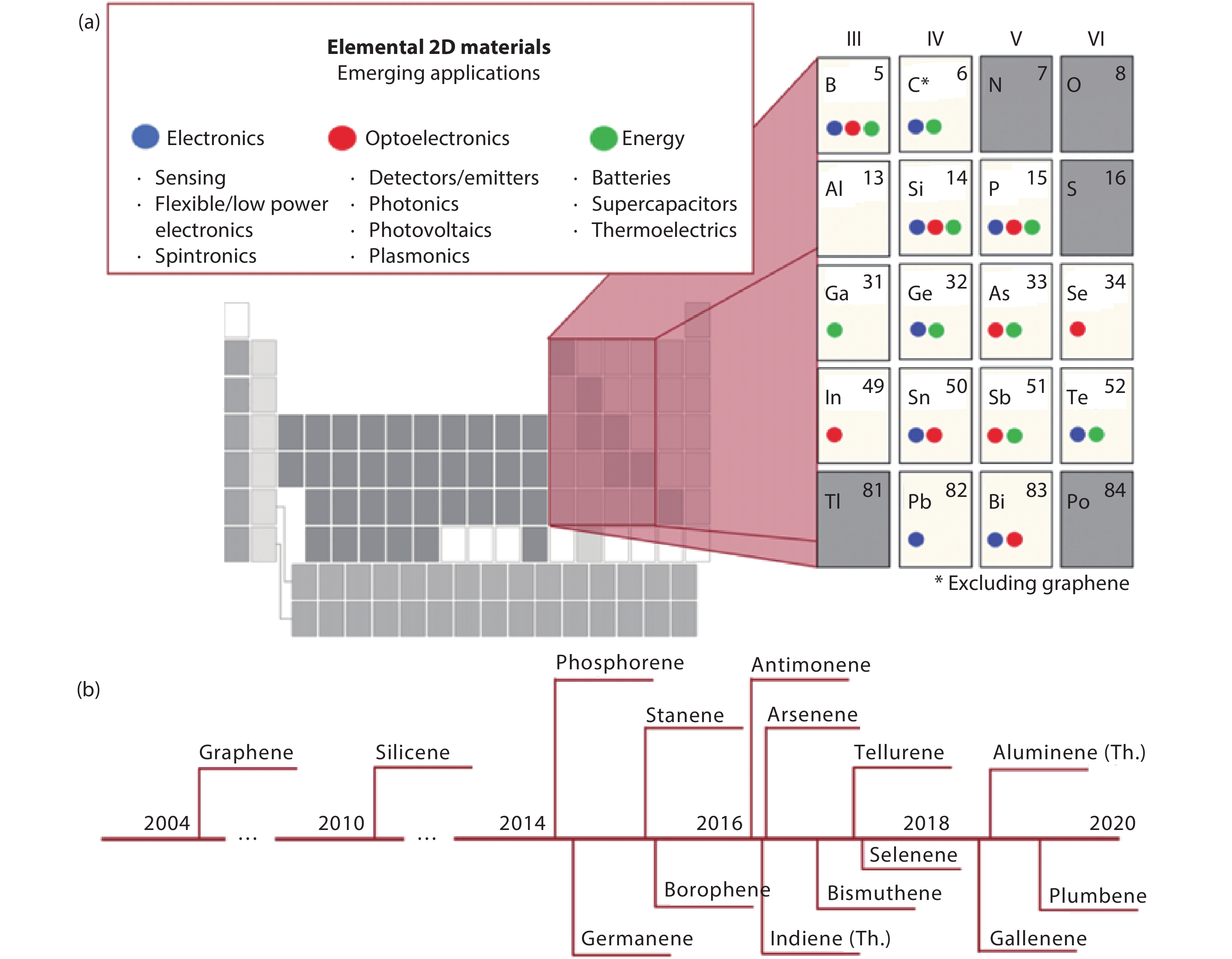
Two-dimensional (2D) materials with atomic thickness demonstrate unique physical, chemical and mechanical characteristics against the corresponding three-dimensional (3D) forms. They could also be further modified by other means, such as nanostructuring, doping, twisting, etc. These provide new potential in the applicants of electronics, optoelectronics and energy storage devices, superconductors, etc. Hence, the research on 2D materials experienced an explosive growth since the pioneering work on graphene[
To our best knowledge, 15 types of elemental 2D materials in main group have been experimentally realized or theoretically predicted. They include borophene[
![]()
Figure 1.(Color online) (a) Overview of 2D elemental main group materials and (b) the corresponding timeline of experimental realization, where “Th.” represents only theoretical prediction
Tellurene is the 2D form of tellurium in group-VIA, which was proposed by theoretical calculations and then verified by experiments in 2017. Unlike other 2D MLs, such as graphene, tellurene has no layered counterparts. Its formation mechanism is the strain caused by competition between its multivalency and helical chain in the low-dimensional case. Tellurene has favourable properties such as high carrier mobility, excellent light absorption, superb thermoelectric performance and good stability at room temperature, which has great potential in nanodevices. Thus tellurene has aroused intensive attention since its advent. This review aims to summarize the latest progress and research status on tellurene. The review has been organized into five sections as follows. In the first section, the 2D material family as a whole is briefly discussed. In the second section, we review the theoretical prediction and experimental synthesis of tellurene. The excellent properties of tellurene are summarized in the third section. The fourth section presents the performance modulation of tellurene as well as its functionalization. In the last section, we make some prospects to the future development of tellurene.
2. Rise of tellurene
Since the elemental 2D MLs in group-IIIA, -IVA and -VA have been developed, scientists began to challenge the possibility of group-VIA single element forming 2D atomic crystals. Structurally, the bulk structures of group-VIA are mostly chain-like, not the van der Waals (vdW) layered structure like graphite. Chemically, for the group-VIA elements (S, Se, Te), the difference of the absolute value of their oxidation states (+6 and –2) is larger than those in group-IIIA, -IVA and -VA. So, the existence of group-VIA 2D elemental MLs is a scientifically interesting and challenging issue. 3D is the source and foundation of 2D, and thus we firstly trace back to the crystal structure of 3D Te bulk together with its typical characteristics.
2.1. Te in bulk phase
In group-VIA, the nonmetallic element Te is located between the nonmetallic element Se and the metal element Po, which determines the metalloid property of Te. The most stable structure of Te at the room pressure is a trigonal one termed as Te-I, consisting of helical chains parallel to the c-axis, which run along the c-axis and are arranged in a hexagonal form. In the helical chain, each one third of atoms are straightly above other atoms, so that the projected plane of the chain forms an equilateral triangle (see Fig. 2(a)). Intrachain Te atoms are bound by covalent bonds through a helical turn of 120º in [0001] direction while interchain atoms are noncovalently bonded[
![]()
Figure 2.(Color online) (a) Top view of crystal structure of Te-I as well as its helical chains of Te atoms run in righ- and left-hand manners. (b–d) different crystal structures of Te bulk under high pressure. (e) Band structures of Te-I[
Te-I is a semiconductor with the bandgap of 0.35 eV[
Like natural organic substances such as sugar, the Te-I bulk with the helical structure is a chiral crystal due to lack of mirror symmetry and inversion center, which has the inequivalent right- and left-handed structures with the space groups of P3121 and P3221 (see Fig. 2(a)), respectively. The chiral tellurium is suitable for engineering owing to the simplest crystal structure, which has received particular attention[
The bulk Te also has diverse phases under high pressure[
2.2. Advent of 2D tellurene
By combining the particle-swarm optimization searches[
![]()
Figure 3.(Color online) Crystal structures and total charge densities of three kinds of tellurene, as well as the electronic band structure and optical absorption of
The theoretical work on the group-VIA 2D ML tellurene published attracted wide interest of scholars. Now, it has been four years since the firstly submitted 2D tellurene manuscript on arXiv platform in January 2016, and there have been a great many studies on the experimental preparation, property study and application exploration of tellurene. Herein, we will review these studies, hoping to introduce newcomers to the field of tellurene and stimulating their interest.
2.3. Prediction of multiple 2D tellurene structures
In view of the multivalency induced diverse phases of bulk Te under high-pressure[
By artificially compressing a 2D assembly of the native helices in the normal direction of the 2D layer, Liu et al. obtained abnormally stable 2D δ-Te as well as δ-Se. And the stable η-phase is obtained by a series of reflections of δ-structure with fixing the bond lengths and bond angles constant. δ- and η-Te are indirect and direct semiconductors with the bandgap of 0.9 and 0.3 eV, respectively[
![]()
Figure 4.(Color online) Te ML structures: (a)
Using DFT methods, Jiang et al. proposed a class of novel 2D tellurenyne MLs composed of atomic Te chains through noncovalent bonds[
Besides the tellurene MLs mentioned above, some 2D Te few-layer (FL) structures with excellent properties have been found[
![]()
Figure 5.(Color online) Three-layer
These 2D FL Te can be originated from the reconstitution of crystal surfaces of trigonal Te-I. Both γ-phase and ε-phase can be obtained by cutting along the [0001] direction. β-phase and δ-phase can be formed by cutting along the [1010] and [1120] directions, respectively[
For 2D α- and β-phase FL tellurene, further studies have found that it can be stabilized by hole or electron doping[
Based on first-principles calculations, Wu et al. designed a highly kinetic stable layered Te bulk structure named β-Te bulk, like other layered bulk materials such as graphite. Bulk β-Te is a semiconductor with the bandgap of 0.325 eV, whose ML structure is 2D β-Te[
The diverse 2D structures of tellurene not only enrich the 2D material family, but also provide candidates to meet the different functions for electronics.
2.4. Experimental synthesis
The purpose of exploring 2D materials with excellent performances is their massive applications in highly integrated 2D devices. To this end, it is crucial to realize the experimental preparation of large-size 2D materials with uniform characteristics. Owing to the intrinsic structural anisotropy, 1D Te nanostructures were predominantly yielded by previously reported synthetic methods[
The top–down mechanical exfoliation method plays a pioneering role in discovering 2D MLs, which is still adopted to fabricate tellurene. Churchill et al. exfoliated ultra-thin Te flakes from trigonal Te single crystal, with the thicknesses ranging from 1 to 2 nm and the widths smaller than 100 nm[
By a substrate-free solution process or hydrothermal method, Ye et al. fabricated free-standing, large-area and high-quality ML and FL tellurene, and the tellurene-based transistors can be stable for over two months at room temperature, also presenting the excellent properties including high on/off ratios, large current densities and high carrier mobilities[
![]()
Figure 6.(Color online) (a) Large-area 2D tellurene obtained from solution-grown method and material characterization[
Vapor deposition is one of the main methods for preparing thin film materials. It has been proved that physical vapor deposition method (PVD) including molecular beam epitaxy (MBE) is also employed to produce 2D tellurene. Guo et al. obtained β-tellurene ML and FL thickness by MBE on the graphene/6H-SiC(0001) substrate[
Using horizontal PVD method, Tongay et al. revealed that highly crystalline and self-oriented tellurene sheets can be grown on the GaS and GaSe vdW surfaces resulting from the much-reduced total energy and a stronger degree of coupling between adjacent layers[
In addition to the above exfoliation method, solution method and vapor deposition method, some other preparation methods of tellurene have been developed. For instance, Wu et al. achieved ultrathin Te film with large area and clean interface through a topotactic transformation, where 2D Te structure came from layered MTe2 (M = Ti, Mo, W, etc.) matrix by the excessive lithiation[
3. Performance and applications of tellurene
Tellurene is an outstanding 2D elemental material, which simultaneously overcomes the shortcomings such as the zero-bandgap of graphene, the instability of BP in air condition, and the small carrier mobility of MoS2. The measures on tellurene properties have been explored.
3.1. Mechanical properties
He et al. studied the strain-induced mechanical property variations in ML tellurene using first-principles calculations[
3.2. Thermoelectric characteristics
Due to a high value of thermoelectric figure-of-merit ZT, trigonal Te bulk is considered to be a remarkable thermoelectric material. In the light of recent progresses in the synthesis route of 2D tellurene films together with the increasing trend of utilizing nano thermoelectric devices, there is a growing interest in the thermoelectric properties of 2D tellurene.
Based on first-principles calculations and phonon Boltzmann transport, Ren and Liu et al. revealed the ultralow thermal properties in the ML β-Te, shown in Fig. 7(a)[
![]()
Figure 7.(Color online) (a) Lattice thermal conductivity of tellurene versus temperature[
Chai et al. showed the three-phonon limited thermal conductivity of both square selenene and tellurene by DFT calculations[
3.3. Ferroelectric properties
Due to far-reaching implications in industrial application, ferroic materials have been one of the most important topics in condensed matter physics. The rapid development of 2D materials makes it provide unique 2D ferroelectric property due to the quantum confinement.
Although 2D Te ML structure has no ferroelectricity, the strong ferroelectricity in 2D Te FL (based on the named rule of space group) is introduced by spontaneous in-plane polarization owing to the interlayer interaction of lone pairs (see Fig. 8)[
![]()
Figure 8.(Color online) Differential charge density and spin-texture of bilayer Te phases[
Based on DFT, strain can induce the transition from β-Te ML with centrosymmetry to α-Te ML without centrosymmetry. Meanwhile, 2D ferroelectrics can form, in which the magnitude of polarization can reach up to about 90 μC/cm2 by a tensile strain, resulting in a giant piezoelectric effect that is two orders of magnitude stronger than that of MoS2 ML[
3.4. Transport properties
Normally, the electron and hole transportations along the chemical bond direction are much faster than those along the other directions in anisotropic materials. However, due to the delocalized lone pair electrons, Liu et al. observed that intrachain and interchain directions exhibit nearly isotropic electrical transport in trigonal Te composed of helical atomic chains, which originates from similar effective masses and potentials of charge carriers in different transporting directions[
Due to the striking characters, 2D tellurene is deemed to be a promising channel candidate of post-silicon FETs. By performing exact ab-initio quantum transport simulations, the performance limits of sub-5-nm ML tellurene metal–oxide–semiconductor FETs (MOSFETs) were explored. It was found that the optimized p-type ML tellurene MOSFET satisfies both the high performance and low power which the International Technology Roadmap for Semiconductors requires at a gate length of 4 nm with a negative capacity dielectric (see Figs. 9(a)–9(c))[
![]()
Figure 9.(Color online) (a) Schematic view of the double-gated ML tellurene MOSFET. (b, c) Transfer characteristics of the corresponding MOSFETs with 5 nm gate length[
Quantum Hall effect (QHE) is a macroscopic manifestation of quantized states only occurring in confined 2D electron gas (2DEG) systems. At low temperature, QHE is experimentally hosted in the 2DEG with high-mobility and large external magnetic field. Due to the easy accessibility of thin films with the thickness of ML or FL at the 2D quantum limit, 2D vdW materials are considered to be interesting material systems for studying quantum transport because they could reveal unique host material properties. Ye et al. for the first time directly observed QHE in the thin 2D tellurene films synthesized by hydrothermal method, which present high-quality and high hole mobility of nearly 3000 cm2V−1s−1 at low temperatures. The interplay between the Zeeman effect and SOC causes anomalies in both temperature-dependent oscillation amplitudes and transport characteristics (see Fig. 9(d))[
Based on solution-grown tellurene flakes with the thickness < 30 nm, Frisbie et al. fabricated and characterized high-performance electrolyte-gated transistors (EGTs)[
Fascinating properties can be found in atomic chains formed in a spiral shape, such as phases hosting localized bound states in their electronic structure. By the nearest-neighbor tight-binding approximation, strict conditions for a topological phase hosting zero-energy edge-bound modes were identified in a generic single atomic helix[
Nakayama et al. carried out high-resolution angle-resolved photo emission spectroscopy on the trigonal Te composed of helical chains[
Dirac and Weyl nodal materials can host low-energy relativistic quasiparticles. The topological properties of Dirac/Weyl materials can directly manifest through quantum Hall states under strong magnetic fields. However, most Dirac/Weyl nodes generically exist in semimetals without exploitable bandgaps due to their accidental band-crossing origin. Tellurene possesses chiral crystal structure which induces unconventional Weyl nodes with a hedgehog-like radial spin texture near the conduction band edge. Ye et al. experimentally observed Weyl fermions in the synthesize high-quality n-type tellurene by a hydrothermal method with subsequent dielectric doping, and detected a topologically non-trivial π Berry phase in quantum Hall sequences[
Due to Te intrinsic p-type nature, few people experimentally studied its conduction band (CB). By atomic layer deposited dielectric doping technique, the CB transport properties of 2D Te can be accessed in a controlled fashion. In n-type 2D Te films, Ye et al. performed a systematic study on the weak-antilocalization (WAL) effect[
Using many-body perturbation theory based on first-principles, Lu et al. investigated the evolvement of the relationship between quasipartile energies and excitons evolving as the dimensionality of Te nanostructures changes[
3.5. Optical properties
2D tellurene is a promising and versatile material, which offers a platform for mid-infrared photonics. The waveguide-integrated tellurene photodetector and Pockels effect modulator were designed (See Fig. 10(a))[
![]()
Figure 10.(Color online) (a) Diagram of waveguide integrated tellurene photodetector, in which the inset is top view of crystal structure of tellurene along [0001] axis[
Nonlinear optics is widely used in laser, information and material technologies. 2D nanomaterials have excellent wide-band nonlinear saturation absorption properties, which can be made into the saturable absorber (SA) of Q-switched and mode-locked fiber lasers producing different wavelength pulses, such as graphene[
Firstly, as a result of the strong interaction between light and matter from visible to infrared range, the unique 2D Te-based nonlinear photonic device with room temperature stability can act as photonic diode and all-optical switcher[
Solution-synthesized Te nanoflakes can be used as short-wave infrared photodetectors[
Through DFT combined with the nonequilibrium Green’s function calculation, Gao et al. found that tellurene bilayer presents a broad photoelectric response over the range from visible to near-infrared region[
By studying ambipolar tellurene based FETs, Berweger demonstrated the general ability of near-field scanning microwave microscopy to image and study the local carrier type and relevant conductivity by operando[
4. Performance modulations of tellurene
4.1. Strain effects
Strain-engineering on 2D semiconductors could further tailor their electronic properties. The strain effect on 2D tellurene with the helical chain as basic unit can induce phase transition and some exotic natures.
Based on DFT, it was manifested that the strain-induced phase transition from a centrosymmetric β-phase to a non-centrosymmetric α-phase in ML tellurene (named based on space group, and next paragraph is the same)[
Leng et al. showed that in-plane compression facilitates the α→β phase transition, whereas in-plane tensile strains invariably enable α-phase to be more stable than β-phase[
Yang et al. demonstrated by first-principles DFT that strain-engineering can controll the highly anisotropic electron mobility and electrical conductance of β-Te[
![]()
Figure 11.(Color online) (a) Electrical conductance of
Through experimental demonstrations of 1D vdW Te by Raman spectroscopy under strain and magneto-transport, pronounced strain response along the c-axis and no strain response along the a-axis were observed due to the strong intrachain covalent bonds and the weak interchain vdW interaction, respectively. And magneto-transport results also confirmed its anisotropic property, resulting in obviously different magneto-resistance behaviors in three different magnetic field directions. Specifically, phase coherence length of Lϕ ≈ T−0.5 was obtained from weak antilocalization effect, indicating its 2D transport characteristics under an applied magnetic field normal to the thin film. By comparison, Lϕ ≈ T−0.33 from universal conductance fluctuations was obtained under the magnetic field in the c-axis, which indicated its 1D transport nature along the helical chain. From experimental perspectives, the 1D vdW structure is strongly evidenced by these studies obtained from the single crystal Te thin film with high quality[
4.2. Defect effect
Due to the atomic level dimension, the effects of vacancies and common adsorbates in ambient conditions and functional group play a significant role in 2D material based devices.
A comprehensive study on the adsorption of nineteen typical adatoms and five typical molecules of H2, O2, H2O, NO2, and NH3 adsorbed above ML α-Te and β-Te using first-principles based on DFT could be found in Ref. [103]. It was revealed that diverse electronic states can be induced by these adatoms, such as n-type doping, p-type doping, half-metal, and spin-gapless semiconductor features. The molecules of H2O and O2 behave essentially different on tellurene, and water adsorption can be evidently enhanced by adjacent pre-adsorbed O2, shown in Fig. 12(a)[
![]()
Figure 12.(Color online) (a) Adsorption configurations of H2O and energy barriers for dissociation of O2 on the tellurene surface[
Performing DFT and molecular dynamics simulations, Ataca et al. investigated the stabilities and electronic properties of α- and β-tellurene ML as well as the corresponding H, O, and F functionalized counterparts, including SOC effects[
Chemiresistive sensor devices made from 2D materials have been extensively investigated. Neverthless, no single material has all the desirable attributes until the discovery of tellurene. The puckered structure of tellurene offers Te atoms different coordination environments on the surface, which would be propitious to sense. Wang et al. found that tellurene succeeds in a sensor for detecting NO2 (See Fig. 12(b))[
Due to the high chemical stability and excellent electrical characteristics, SF6 has been widely used in gas insulated switchgear. Whereas the electric arc and corona can normally decompose SF6, generating HF, SOF2, SO2, SO2F2, H2S, etc., which could corrode the medium in the ninternal equipment[
4.3. Te nanostructures
Like other nanoribbons obtained from 2D material, the stabilities of both ML and bilayer tellurene nanoribbons (TNRs) mainly depend on their widths[
![]()
Figure 13.(Color online) (a) Top and side views of the crystal structures for ML tellurene, and tip, notch, and chain nanoribbons, respectively. The letter
Owing to the bonding free surface carrier transport, 2D materials possess application prospect in semiconductor logic devices. However, the edge issues induced by scaling transistor width have notably restricted their surface transport in the lateral direction, causing the increase of effective mass and the bandgap fluctuating. Consequently, it is of importance to find a novel 2D material with both excellent surface transport and free of edge effect. In view of the distinctive Te–Te bonds in tellurene, the edge effect on the transport properties was theoretically studied via TNRs with four types of edge[
The anomalous phase transition induced by pressure was observed in the single crystalline TNRs with high quality obtained from hydrothermal method[
Electrically manipulating charge carriers supports the operations of state-of-the-art devices. However, for charge carriers, effectively controlling interfacial energetics by the dynamic mechanical stimuli has been rarely unexplored for semiconductor nanodevices, which can be addressed by exciting opportunities offered by piezotronic effect in nanostructured piezoelectric semiconductors. Gao et al. for the first time explored piezotronic effect in p-type Te nanobelt experimentally and systematically investigated the strain-gated charge carriers transport properties[
4.4. Te-based heterostructures
Heterostructures by stacking two or more 2D ML materials together in transverse or longitudinal manner can provide new potentiality beyond its single ML materials[
In virtue of its desirable optoelectronic properties, high stability and strong visible light absorption, tellurene is considered as a promising candidate for the design of highly efficient heterojunction solar cells. Using first-principles calculations, it was found that Te/TMD vdWH presents an ideal bandgap of 1.47 eV as well as other excellent optoelectronic properties, such as the strong visible light absorption up to 5.0 × 105 cm−1 and the high carrier mobility up to 2.87 × 103 cm2V−1s−1 (Fig. 14(a))[
![]()
Figure 14.(Color online) (a) Geometric structures of Te/XS2, Te/XSe2 and Te/XTe2 (X = Mo or W) vdWHs (top views), and diagram of power conversion efficiency of solar cells made from Te/TMDs vdWH[
The graphene (G)/α-Te and G/β-Te interface are formed by an n-type Schottky contact with a negligible Schottky barrier height (SBH) and a p-type Schottky contact with a SBH of 0.51 eV, respectively[
Using first-principles, the electronic and optical properties were investigated for the α-Te-based vertical vdWHs constructed by α-Te and some other 2D MLs including MoS2[
5. Summary and perspective
We have reviewed the theoretical and experimental works related to 2D tellurene since it was proposed by our theoretical simulations. Unlike other 2D materials with the corresponding 3D layered bulk phases, 2D tellurene has been invented in a building-a-lego-like manner. We have revealed all possible phases, different combination multilayer stackings, nanoengineering, defects and heterostructures, etc. Each will lead to its own interesting properties, which provide more options for electronic applications. Their mechanical, thermal, electronic and tranport properties have been reviewed along with the experimental realization of electronic applications combined with theoretical predictions. It outstands other 2D materials, which makes it a promising candidate for next-generation nanodevices.
It is of great importance to theoretically design more 2D structures of Tellurene as well as explore their formation mechanism, excellent properties and applications, especially the unique properties such as transport, magnetism and superconductivity. Secondly, it is still necessary to study the functionalization of the tellurene phases which have been successfully prepared by experiments, through defects, strains, heterostructures and nanoribbons, etc. The performance of the device is dependent on not only the materials but also the fabrication procedures, such as nanosheet transfer, substrates and contacts metals. Hence, the standardization of fabrication procedures is also critical, which is the common problem for all the 2D material-based devices. For the synthesis of 2D tellurene, it is still on the way to high quality, large dimension, and massive production monolayer, which will be the bottleneck for its further massive device production.
2D tellurene provides an excellent example how theoretical calculations play the leading role in the materials discovery followed by experimental realization, even for the conventional main group element. And the research on big-data driven process-structure-property relationship will further inspire the collective efforts for open questions and improvements in the 2D tellurene as well as 2D material science in general.
Acknowledgements
This work was supported partly by the National Natural Science Foundation of China (Grant Nos. 11804082 and 11774078), by the Foundation of Henan Educational Committee (Grant No. 18A140018), and by the Doctoral Foundation of Henan Polytechnic University (B2018-37).
References
[1] K S Novoselov. Electric field effect in atomically thin carbon films. Science, 306, 666(2004).
[2] B J Feng, J Zhang, Q Zhong et al. Experimental realization of two-dimensional boron sheets. Nat Chem, 8, 563(2016).
[3] C Kamal, A Chakrabarti, M Ezawa. Aluminene as highly hole-doped graphene. New J Phys, 17, 083014(2015).
[4] M L Tao, Y B Tu, K Sun et al. Gallenene epitaxially grown on Si(111). 2D Mater, 5, 035009(2018).
[5] D Singh, S K Gupta, I Lukačević et al. Indiene 2D monolayer: A new nanoelectronic material. RSC Adv, 6, 8006(2016).
[6] P Vogt, P de Padova, C Quaresima et al. Silicene: compelling experimental evidence for graphenelike two-dimensional silicon. Phys Rev Lett, 108, 155501(2012).
[7] E Bianco, S Butler, S S Jiang et al. Stability and exfoliation of germanane: A germanium graphane analogue. ACS Nano, 7, 4414(2013).
[8] F F Zhu, W J Chen, Y Xu et al. Epitaxial growth of two-dimensional stanene. Nat Mater, 14, 1020(2015).
[9] J Yuhara, B J He, N Matsunami et al. Graphene's latest cousin: Plumbene epitaxial growth on a “nano WaterCube”. Adv Mater, 31, 1901017(2019).
[10] L K Li, Y J Yu, G J Ye et al. Black phosphorus field-effect transistors. Nat Nanotechnol, 9, 372(2014).
[11] S L Zhang, Z Yan, Y F Li et al. Atomically thin arsenene and antimonene: Semimetal-semiconductor and indirect-direct band-gap transitions. Angew Chem Int Ed, 54, 3112(2015).
[12] J P Ji, X F Song, J Z Liu et al. Two-dimensional antimonene single crystals grown by van der Waals epitaxy. Nat Commun, 7, 13352(2016).
[13] F Reis, G Li, L Dudy et al. Bismuthene on a SiC substrate: A candidate for a high-temperature quantum spin Hall material. Science, 357, 287(2017).
[14] Z L Zhu, X L Cai, S Yi et al. Multivalency-driven formation of Te-based monolayer materials: A combined first-principles and experimental study. Phys Rev Lett, 119, 106101(2017).
[15] N R Glavin, R Rao, V Varshney et al. Emerging applications of elemental 2D materials. Adv Mater, 32, 1904302(2020).
[16] J S Qiao, Y H Pan, F Yang et al. Few-layer tellurium: One-dimensional-like layered elementary semiconductor with striking physical properties. Sci Bull, 63, 159(2018).
[17] S Q Deng, J Koehler, A Simon. Unusual lone pairs in tellurium and their relevance for superconductivity. Angew Chem Int Ed, 45, 599(2006).
[18] A Coker, T Lee, T P Das. Investigation of the electronic properties of tellurium: Energy-band structure. Phys Rev B, 22, 2968(1980).
[19] M Hulin. Electron band structure of tellurium. J Phys Chem Solids, 27, 441(1966).
[20] R E Beissner. Electron energy bands in tellurium. Phys Rev, 145, 479(1966).
[21] H G Junginger. Electronic band structure of tellurium. Solid State Commun, 5, 509(1967).
[22] M H Weiler. Landau levels in the valence band of tellurium. Solid State Commun, 8, 1017(1970).
[23] D Thanh. Effective mass approximation for acceptors in tellurium. Solid State Commun, 9, 631(1971).
[24] H Shinno, R Yoshizaki, S Tanaka et al. Conduction band structure of tellurium. J Phys Soc Jpn, 35, 525(1973).
[25] R Enderlein, A Hache. Valence and conduction band structure and infrared optical properties of tellurium in the presence of pressure. Phys Status Solidi B, 60, 739(1973).
[26] L A Agapito, N Kioussis, W A Goddard et al. Novel family of chiral-based topological insulators: Elemental tellurium under strain. Phys Rev Lett, 110, 176401(2013).
[27] S Q Lin, W Li, Z W Chen et al. Tellurium as a high-performance elemental thermoelectric. Nat Commun, 7, 10287(2016).
[28] Y Akahama, N Okawa, T Sugimoto et al. Coexistence of a metastable double hcp phase in bcc–fcc structure transition of Te under high pressure. Jpn J Appl Phys, 57, 025601(2018).
[29] Y Tanaka, S P Collins, S W Lovesey et al. Determination of the absolute chirality of tellurium using resonant diffraction with circularly polarized X-rays. J Phys Condens Matter, 22, 122201(2010).
[30] M Hirayama, R Okugawa, S Ishibashi et al. Weyl node and spin texture in trigonal tellurium and selenium. Phys Rev Lett, 114, 206401(2015).
[31] K Nakayama, M Kuno, K Yamauchi et al. Band splitting and Weyl nodes in trigonal tellurium studied by angle-resolved photoemission spectroscopy and density functional theory. Phys Rev B, 95, 125204(2017).
[32] M Sakano, M Hirayama, T Takahashi et al. Radial spin texture in elemental tellurium with chiral crystal structure. Phys Rev Lett, 124, 136404(2020).
[33] Z Y Dong, Y H Ma. Atomic-level handedness determination of chiral crystals using aberration-corrected scanning transmission electron microscopy. Nat Commun, 11, 1588(2020).
[34]
[35] S S Kabalkina, L F Vereshchagin, B M Shulenin. Phase transitions in tellurium at high pressures. J Exp Theor Phys, 45, 2073(1964).
[36] J C Jamieson, D B McWhan. Crystal structure of tellurium at high pressures. J Chem Phys, 43, 1149(1965).
[37] K Aoki, O Shimomura, S Minomura. Crystal structure of the high-pressure phase of tellurium. J Phys Soc Jpn, 48, 551(1980).
[38] Y Akahama, M Kobayashi, H Kawamura. Pressure-induced superconductivity and phase transition in selenium and tellurium. Solid State Commun, 84, 803(1992).
[39] Y C Wang, J Lv, L Zhu et al. Crystal structure prediction via particle-swarm optimization. Phys Rev B, 82, 094116(2010).
[40] E J Reed. Two-dimensional tellurium. Nature, 552, 40(2017).
[41]
[42] D Liu, X Q Lin, D Tománek. Microscopic mechanism of the helix-to-layer transformation in elemental group VI solids. Nano Lett, 18, 4908(2018).
[43] L D Xian, Paz A Pérez, E Bianco et al. Square selenene and tellurene: Novel group VI elemental 2D materials with nontrivial topological properties. 2D Mater, 4, 041003(2017).
[44] W Zhang, Q S Wu, O V Yazyev et al. Topological phase transitions driven by strain in monolayer tellurium. Phys Rev B, 98, 115411(2018).
[45] T Paulauskas, F G Sen, C Sun et al. Stabilization of a monolayer tellurene phase at CdTe interfaces. Nanoscale, 11, 14698(2019).
[46] L J Qi, J Han, W Gao et al. Monolayer tellurenyne assembled with helical telluryne: Structure and transport properties. Nanoscale, 11, 4053(2019).
[47] Y Wang, C C Xiao, M G Chen et al. Two-dimensional ferroelectricity and switchable spin-textures in ultra-thin elemental Te multilayers. Mater Horiz, 5, 521(2018).
[48] C Wang, X Y Zhou, J S Qiao et al. Charge-governed phase manipulation of few-layer tellurium. Nanoscale, 10, 22263(2018).
[49] Y Xiang, S J Gao, R G Xu et al. Phase transition in two-dimensional tellurene under mechanical strain modulation. Nano Energy, 58, 202(2019).
[50] B Z Wu, X H Liu, J R Yin et al. Bulk
[51] Y J Zhu, X L Hu, W W Wang. Poly(vinylpyrrolidone): a new reductant for preparation of tellurium nanorods, nanowires, and tubes from TeO2. Nanotechnology, 17, 645(2006).
[52] H S Qian, S H Yu, J Y Gong et al. High-quality luminescent tellurium nanowires of several nanometers in diameter and high aspect ratio synthesized by a poly (vinyl pyrrolidone)-assisted hydrothermal process. Langmuir, 22, 3830(2006).
[53] M Mo, J Zeng, X Liu et al. Controlled hydrothermal synthesis of thin single-crystal tellurium nanobelts and nanotubes. Adv Mater, 14, 1658(2002).
[54] Q S Wang, M Safdar, K Xu et al. Van der Waals epitaxy and photoresponse of hexagonal tellurium nanoplates on flexible mica sheets. ACS Nano, 8, 7497(2014).
[55] W Z Wu, G Qiu, Y X Wang et al. Tellurene: its physical properties, scalable nanomanufacturing, and device applications. Chem Soc Rev, 47, 7203(2018).
[56] H O H Churchill, G J Salamo, S Q Yu et al. Toward single atom chains with exfoliated tellurium. Nanoscale Res Lett, 12, 1(2017).
[57] Y Lin, Y Wu, R Wang et al. Two-dimensional tellurium nanosheets for photoacoustic imaging-guided photodynamic therapy. Chem Commun, 54, 8579(2018).
[58] Z J Xie, C Y Xing, W C Huang et al. Ultrathin 2D nonlayered tellurium nanosheets: Facile liquid-phase exfoliation, characterization, and photoresponse with high performance and enhanced stability. Adv Funct Mater, 28, 1705833(2018).
[59] F Zhang, G W Liu, Z P Wang et al. Broadband nonlinear absorption properties of two-dimensional hexagonal tellurene nanosheets. Nanoscale, 11, 17058(2019).
[60] J Guo, J L Zhao, D Z Huang et al. Two-dimensional tellurium-polymer membrane for ultrafast photonics. Nanoscale, 11, 6235(2019).
[61] Y Wang, G Qiu, R Wang et al. Field-effect transistors made from solution-grown two-dimensional tellurene. Nat Electron, 1, 228(2018).
[62] Y X Wang, R de Souza Borges Ferreira, R X Wang et al. Data-driven and probabilistic learning of the process-structure-property relationship in solution-grown tellurene for optimized nanomanufacturing of high-performance nanoelectronics. Nano Energy, 57, 480(2019).
[63] Y S Chen, J Ding, X M He et al. Synthesis of tellurium nanosheet for use in matrix assisted laser desorption/ionization time-of-flight mass spectrometry of small molecules. Microchim Acta, 185, 1(2018).
[64] M Gao, X W Wang, Y Z Hong et al. One-pot hydrothermal synthesis of thin tellurene nanosheet and its formation mechanism. J Nanomater, 2019, 1(2019).
[65] X C Huang, J Q Guan, Z J Lin et al. Epitaxial growth and band structure of Te film on graphene. Nano Lett, 17, 4619(2017).
[66] J L Chen, Y W Dai, Y Q Ma et al. Ultrathin
[67] S Khatun, A Banerjee, A J Pal. Nonlayered tellurene as an elemental 2D topological insulator: Experimental evidence from scanning tunneling spectroscopy. Nanoscale, 11, 3591(2019).
[68] S Yang, B Chen, Y Qin et al. Highly crystalline synthesis of tellurene sheets on two-dimensional surfaces: Control over helical chain direction of tellurene. Phys Rev Mater, 2, 104002(2018).
[69] A Apte, E Bianco, A Krishnamoorthy et al. Polytypism in ultrathin tellurium. 2D Mater, 6, 015013(2018).
[70] J Peng, Y Pan, Z Yu et al. Two-dimensional tellurium nanosheets exhibiting an anomalous switchable photoresponse with thickness dependence. Angew Chem Int Ed, 57, 13533(2018).
[71] Y L Dong, B W Zeng, X J Zhang et al. Study on the strain-induced mechanical property modulations in monolayer Tellurene. J Appl Phys, 125, 064304(2019).
[72] Z B Gao, F Tao, J Ren. Unusually low thermal conductivity of atomically thin 2D tellurium. Nanoscale, 10, 12997(2018).
[73] S Sharma, N Singh, U Schwingenschlögl. Two-dimensional tellurene as excellent thermoelectric material. ACS Appl Energy Mater, 1, 1950(2018).
[74] G Liu, Z B Gao, J Ren. Anisotropic thermal expansion and thermodynamic properties of monolayer
[75] G Qiu, S Y Huang, M Segovia et al. Thermoelectric performance of 2D tellurium with accumulation contacts. Nano Lett, 19, 1955(2019).
[76] C S Lin, W D Cheng, G L Chai et al. Thermoelectric properties of two-dimensional selenene and tellurene from group-VI elements. Phys Chem Chem Phys, 20, 24250(2018).
[77] K Chang, J W Liu, H C Lin et al. Discovery of robust in-plane ferroelectricity in atomic-thick SnTe. Science, 353, 274(2016).
[78]
[79] X R Cai, Y Y Ren, M H Wu et al. Strain-induced phase transition and giant piezoelectricity in monolayer tellurene. Nanoscale, 12, 167(2020).
[80] Y Y Liu, W Z Wu, W A III Goddard. Tellurium: fast electrical and atomic transport along the weak interaction direction. J Am Chem Soc, 140, 550(2018).
[81] J H Yan, H Pang, L Xu et al. Excellent device performance of sub-5-nm monolayer tellurene transistors. Adv Electron Mater, 5, 1900226(2019).
[82] G Qiu, Y Wang, Y Nie et al. Quantum transport and band structure evolution under high magnetic field in few-layer tellurene. Nano Lett, 18, 5760(2018).
[83] X L Ren, Y Wang, Z T Xie et al. Gate-tuned insulator–metal transition in electrolyte-gated transistors based on tellurene. Nano Lett, 19, 4738(2019).
[84] P K Li, J D Sau, I Appelbaum. Robust zero-energy bound states in a helical lattice. Phys Rev B, 96, 115446(2017).
[85] P K Li, I Appelbaum. Intrinsic two-dimensional states on the pristine surface of tellurium. Phys Rev B, 97, 201402(2018).
[86]
[87] C Niu, G Qiu, Y X Wang et al. Gate-tunable strong spin-orbit interaction in two-dimensional tellurium probed by weak antilocalization. Phys Rev B, 101, 205414(2020).
[88] Y Y Pan, S Y Gao, L Yang et al. Dependence of excited-state properties of tellurium on dimensionality: From bulk to two dimensions to one dimensions. Phys Rev B, 98, 085135(2018).
[89] S Deckoff-Jones, Y X Wang, H T Lin et al. Tellurene: A multifunctional material for midinfrared optoelectronics. ACS Photonics, 6, 1632(2019).
[90] Q L Bao, H Zhang, Y Wang et al. Atomic-layer graphene as a saturable absorber for ultrafast pulsed lasers. Adv Funct Mater, 19, 3077(2009).
[91] J Du, Q K Wang, G B Jiang et al. Ytterbium-doped fiber laser passively mode locked by few-layer molybdenum disulfide (MoS2) saturable absorber functioned with evanescent field interaction. Sci Rep, 4, 6346(6346).
[92] Z Q Luo, Y Z Huang, J Weng et al. 1.06
[93] S F Zhang, X Y Zhang, H Wang et al. Size-dependent saturable absorption and mode-locking of dispersed black phosphorus nanosheets. Opt Mater Express, 6, 3159(2016).
[94] L M Wu, W C Huang, Y Z Wang et al. 2D tellurium based high-performance all-optical nonlinear photonic devices. Adv Funct Mater, 29, 1806346(2019).
[95] W F Zhang, G M Wang, F Xing et al. Passively Q-switched and mode-locked erbium-doped fiber lasers based on tellurene nanosheets as saturable absorber. Opt Express, 28, 14729(2020).
[96] M Amani, C L Tan, G Zhang et al. Solution-synthesized high-mobility tellurium nanoflakes for short-wave infrared photodetectors. ACS Nano, 12, 7253(2018).
[97] C F Shen, Y H Liu, J B Wu et al. Tellurene photodetector with high gain and wide bandwidth. ACS Nano, 14, 303(2020).
[98] S Y Gao, C Q Sun, X Zhang. Ultra-strong anisotropic photo-responsivity of bilayer tellurene: A quantum transport and time-domain first principle study. Nanophotonics, 9, 1931(2019).
[99] S Berweger, G Qiu, Y X Wang et al. Imaging carrier inhomogeneities in ambipolar tellurene field effect transistors. Nano Lett, 19, 1289(2019).
[100] J J Wang, Y R Guo, H Shen et al. A first-principles study of strain tuned optical properties in monolayer tellurium. RSC Adv, 9, 41703(2019).
[101] H H Ma, W Hu, J L Yang. Control of highly anisotropic electrical conductance of tellurene by strain-engineering. Nanoscale, 11, 21775(2019).
[102] Y C Du, G Qiu, Y X Wang et al. One-dimensional van der waals material tellurium: Raman spectroscopy under strain and magneto-transport. Nano Lett, 17, 3965(2017).
[103] X H Wang, D W Wang, A J Yang et al. Effects of adatom and gas molecule adsorption on the physical properties of tellurene: A first principles investigation. Phys Chem Chem Phys, 20, 4058(2018).
[104] W P Xu, L Y Gan, R Wang et al. Surface adsorption and vacancy in tuning the properties of tellurene. ACS Appl Mater Interfaces, 12, 19110(2020).
[105] D W Wang, A J Yang, T S Lan et al. Tellurene based chemical sensor. J Mater Chem A, 7, 26326(2019).
[106] D Wines, J A Kropp, G Chaney et al. Electronic properties of bare and functionalized two-dimensional (2D) tellurene structures. Phys Chem Chem Phys, 22, 6727(2020).
[107] D K Liu, Y G Gui, C Ji et al. Adsorption of SF6 decomposition components over Pd (111): A density functional theory study. Appl Surf Sci, 465, 172(2019).
[108] H P Cui, K Zheng, L Q Tao et al. Monolayer tellurene-based gas sensor to detect SF6 decompositions: A first-principles study. IEEE Electron Device Lett, 40, 1522(2019).
[109] Z F Liang, Y Wang, C Q Hua et al. Electronic structures of ultra-thin tellurium nanoribbons. Nanoscale, 11, 14134(2019).
[110] Y Lv, Y Liu, W J Qin et al. Prediction of stable and high-performance charge transport in zigzag tellurene nanoribbons. IEEE Trans Electron Devices, 66, 2365(2019).
[111] H Li, K Wu, S J Yang et al. Anomalous phase transition behavior in hydrothermal grown layered tellurene. Nanoscale, 11, 20245(2019).
[112] S J Gao, Y X Wang, R X Wang et al. Piezotronic effect in 1D van der Waals solid of elemental tellurium nanobelt for smart adaptive electronics. Semicond Sci Technol, 32, 104004(2017).
[113] J Kang, S Tongay, J Zhou et al. Band offsets and heterostructures of two-dimensional semiconductors. Appl Phys Lett, 102, 012111(2013).
[114] J M Liao, B S Sa, J Zhou et al. Design of high-efficiency visible-light photocatalysts for water splitting: MoS2/AlN(GaN) heterostructures. J Phys Chem C, 118, 17594(2014).
[115] Q K Wu, S K Jang, S Park et al.
[116] X R Zhang, Z S Meng, D W Rao et al. Efficient band structure tuning, charge separation, and visible-light response in ZrS2-based van der Waals heterostructures. Energy Environ Sci, 9, 841(2016).
[117] C Si, Z Z Lin, J Zhou et al. Controllable Schottky barrier in GaSe/graphene heterostructure: The role of interface dipole. 2D Mater, 4, 015027(2016).
[118] K Wu, H H Ma, Y Z Gao et al. Highly-efficient heterojunction solar cells based on two-dimensional tellurene and transition metal dichalcogenides. J Mater Chem A, 7, 7430(2019).
[119] X L Cai, X T Jia, Y J Liu et al. Enhanced carrier mobility and tunable electronic properties in α-tellurene monolayer via an α-tellurene and h-BN heterostructure. Phys Chem Chem Phys, 22, 6434(2020).
[120] X M Qin, W Hu, J L Yang. Tunable Schottky and Ohmic contacts in graphene and tellurene van der Waals heterostructures. Phys Chem Chem Phys, 21, 23611(2019).
[121] J H Yan, X Y Zhang, Y Y Pan et al. Monolayer tellurene–metal contacts. J Mater Chem C, 6, 6153(2018).
[122] H Pang, J H Yan, J Yang et al. Bilayer tellurene–metal interfaces. J Semicond, 40, 062003(2019).
[123] W L Zhang, D H Chang, Q Gao et al. Interlayer coupling and external electric field tunable electronic properties of a 2D type-I α-tellurene/MoS2 heterostructure. J Mater Chem C, 6, 10256(2018).
[124] Z Ma, Y S Wang, Y T Wei et al. A type-II C2N/α-Te van der Waals heterojunction with improved optical properties by external perturbation. Phys Chem Chem Phys, 21, 21753(2019).
[125] M M Obeid. Tuning the electronic and optical properties of type-I PbI2/α-tellurene van der Waals heterostructure via biaxial strain and external electric field. Appl Surf Sci, 508, 144824(2020).
[126] W Y Yu, S F Li, X L Cai et al. Ferromagnetic half-metal properties of two dimensional vertical tellurene/VS2 heterostructure: A first-principles study. Comput Mater Sci, 171, 109215(2020).
[127] H L Zhuang, R G Hennig. Stability and magnetism of strongly correlated single-layerVS2. Phys Rev B, 93, 054429(2016).
[128] H R Fuh, C R Chang, Y K Wang et al. Newtype single-layer magnetic semiconductor in transition-metal dichalcogenides VX2 (X = S, Se and Te). Sci Rep, 6, 32625(2016).

Set citation alerts for the article
Please enter your email address
© Copyright 2018-2021 | Chinese Laser Press. All Rights Reserved 沪ICP备15018463号-20