Xiaolin Cai, Xiaoyu Han, Chunxiang Zhao, Chunyao Niu, Yu Jia. Tellurene: An elemental 2D monolayer material beyond its bulk phases without van der Waals layered structures[J]. Journal of Semiconductors, 2020, 41(8): 081002
Search by keywords or author
- Journal of Semiconductors
- Vol. 41, Issue 8, 081002 (2020)
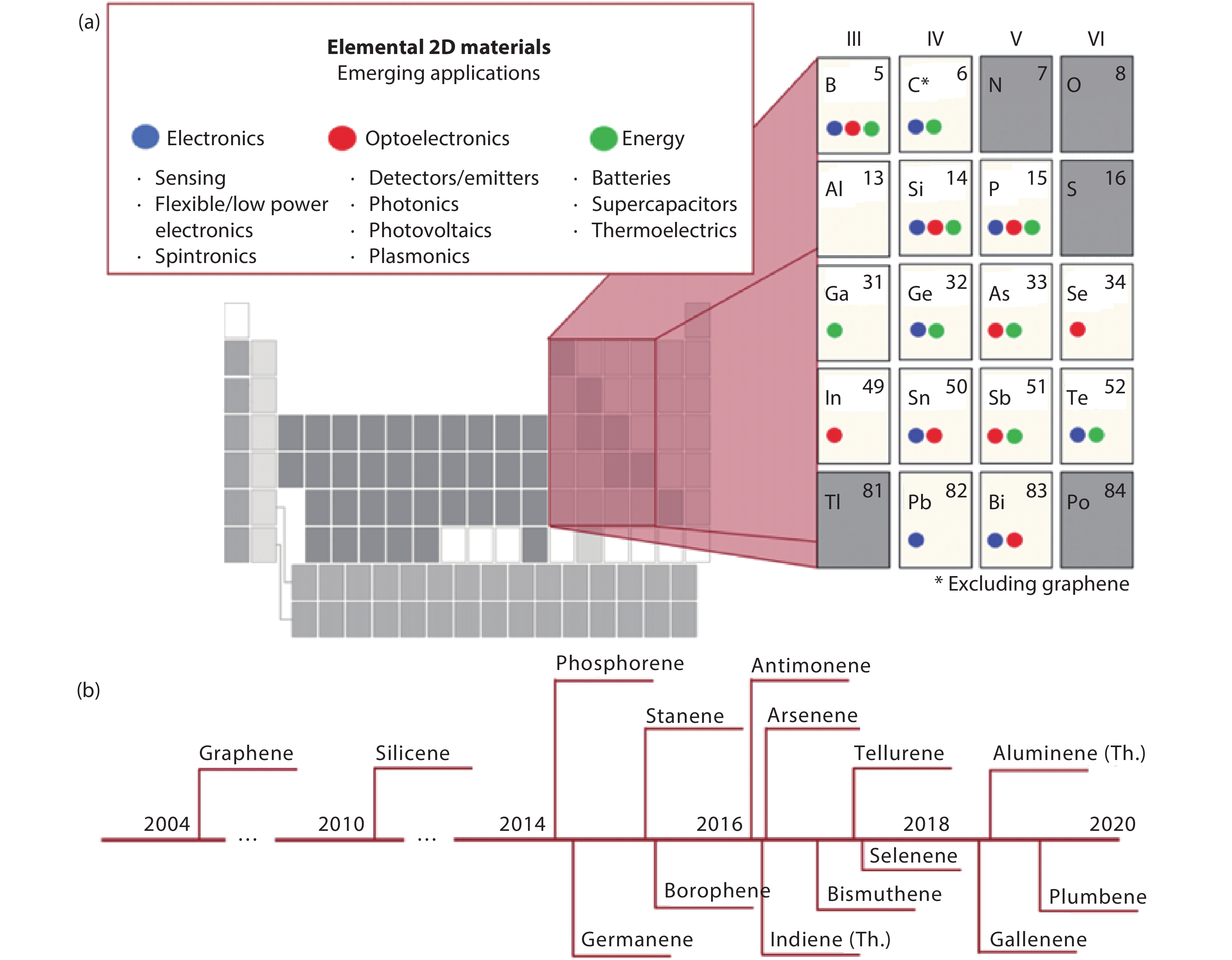
![(Color online) (a) Overview of 2D elemental main group materials and (b) the corresponding timeline of experimental realization, where “Th.” represents only theoretical prediction[15].](/richHtml/jos/2020/41/8/081002/img_1.jpg)
Fig. 1. (Color online) (a) Overview of 2D elemental main group materials and (b) the corresponding timeline of experimental realization, where “Th.” represents only theoretical prediction[15] .
![(Color online) (a) Top view of crystal structure of Te-I as well as its helical chains of Te atoms run in righ- and left-hand manners. (b–d) different crystal structures of Te bulk under high pressure. (e) Band structures of Te-I[26]. (f) Figure of merit (zT) as a function of temperature for p-type ploycrystalline tellurium with different carrier concentrations[27]. (g) Pressure induced phase transition within 0 and 330 GPa[28].](/richHtml/jos/2020/41/8/081002/img_2.jpg)
Fig. 2. (Color online) (a) Top view of crystal structure of Te-I as well as its helical chains of Te atoms run in righ- and left-hand manners. (b–d) different crystal structures of Te bulk under high pressure. (e) Band structures of Te-I[26 ]. (f) Figure of merit (zT ) as a function of temperature for p-type ploycrystalline tellurium with different carrier concentrations[27 ]. (g) Pressure induced phase transition within 0 and 330 GPa[28 ].
Fig. 3. (Color online) Crystal structures and total charge densities of three kinds of tellurene, as well as the electronic band structure and optical absorption of α -Te and β -Te[11 ].
Fig. 4. (Color online) Te ML structures: (a) δ - and η -Te[42 ], (b) square tellurene[43 ], and (c) six types of tellurenyne[46 ].
Fig. 5. (Color online) Three-layer α , β , γ , δ , and ε phases of Te[47 ].
Fig. 6. (Color online) (a) Large-area 2D tellurene obtained from solution-grown method and material characterization[61 ], and (b) topographic images of Te films on graphene[65 ]. (c) Topographic image of an epitaxial Te film as well as the crystal lattice[66 ]. (d) Atomically resolved STM topography of a section of tellurene nanoflake and the corresponding lattice[67 ].
Fig. 7. (Color online) (a) Lattice thermal conductivity of tellurene versus temperature[72 ]. (b) Device structure and pin-out diagram, the experiment setup schematics, and the LIFE current mapping of the real device[75 ].
Fig. 8. (Color online) Differential charge density and spin-texture of bilayer Te phases[47 ].
Fig. 9. (Color online) (a) Schematic view of the double-gated ML tellurene MOSFET. (b, c) Transfer characteristics of the corresponding MOSFETs with 5 nm gate length[81 ]. (d) QHE and SdH oscillations obtained in the 10 nm thick tellurene flake[82 ].
Fig. 10. (Color online) (a) Diagram of waveguide integrated tellurene photodetector, in which the inset is top view of crystal structure of tellurene along [0001] axis[89 ]. (b) HR-TEM image for tellurene nanosheet, and the normalized transmittance as a function of excitation energy density of tellurene nanosheets with different photon energies[59 ]. (c) Characterization of 2D Te nanosheets together with 2D Te/PVP membrane[60 ].
Fig. 11. (Color online) (a) Electrical conductance of β -Te ML under the compressive and tensile strains of -6% and 6%, respectively[101 ]. (b) Lattice structure of trigonal bulk Te as well as the optical image of Te thin film with the thickness of 22.1 nm and two principle lattice orientations on the left. Here, scale bar is 50 μ m. The panel on the right is magneto-resistance of Te thin film as a function of magnetic field Bx at different temperatures[102 ].
Fig. 12. (Color online) (a) Adsorption configurations of H2O and energy barriers for dissociation of O2 on the tellurene surface[104 ]. (b) Schematic and morphological characterization of tellurene based sensors[105 ].
Fig. 13. (Color online) (a) Top and side views of the crystal structures for ML tellurene, and tip, notch, and chain nanoribbons, respectively. The letter t , c and n in ML indicate the tip, chain and notch ribbons, respectively[109 ]. (b) Schematic diagrams of the four edge types in TNRs[110 ].
Fig. 14. (Color online) (a) Geometric structures of Te/XS2, Te/XSe2 and Te/XTe2 (X = Mo or W) vdWHs (top views), and diagram of power conversion efficiency of solar cells made from Te/TMDs vdWH[118 ]. (b) Comparation between the carrier mobilities of the 2D α -tellurene and Te/BN vdWH[119 ].
| |||||||||||||||||||||||||||||||||||||||||||||
Table 1. Elastic stiffness constant Cij , and the ideal tensile stress (ITS) and critical strain (CS) of ML α -, β -, and γ -Te[71 ].

Set citation alerts for the article
Please enter your email address


