
Wenqi Wei, Qi Feng, Zihao Wang, Ting Wang, Jianjun Zhang. Perspective: optically-pumped III–V quantum dot microcavity lasers via CMOS compatible patterned Si (001) substrates[J]. Journal of Semiconductors, 2019, 40(10): 101303
- Journal of Semiconductors
- Vol. 40, Issue 10, 101303 (2019)
Abstract
1. Introduction
With the increasing demand of datacenter and cloud-based applications, large-scale optoelectronic integration is considered as one of the most promising approaches to meet the requirements. By taking advantages of CMOS foundries, silicon photonic technologies are recognized as a major step towards monolithic optoelectronic integration, which has attracted significant attentions[
To realize monolithic epitaxial growth of III–V laser structures on Si substrates, three critical issues must be solved, referring to the materials’ large lattice mismatch, polarities differences and thermal expansion coefficients contrast between III–V epi-layers and group IV substrates.
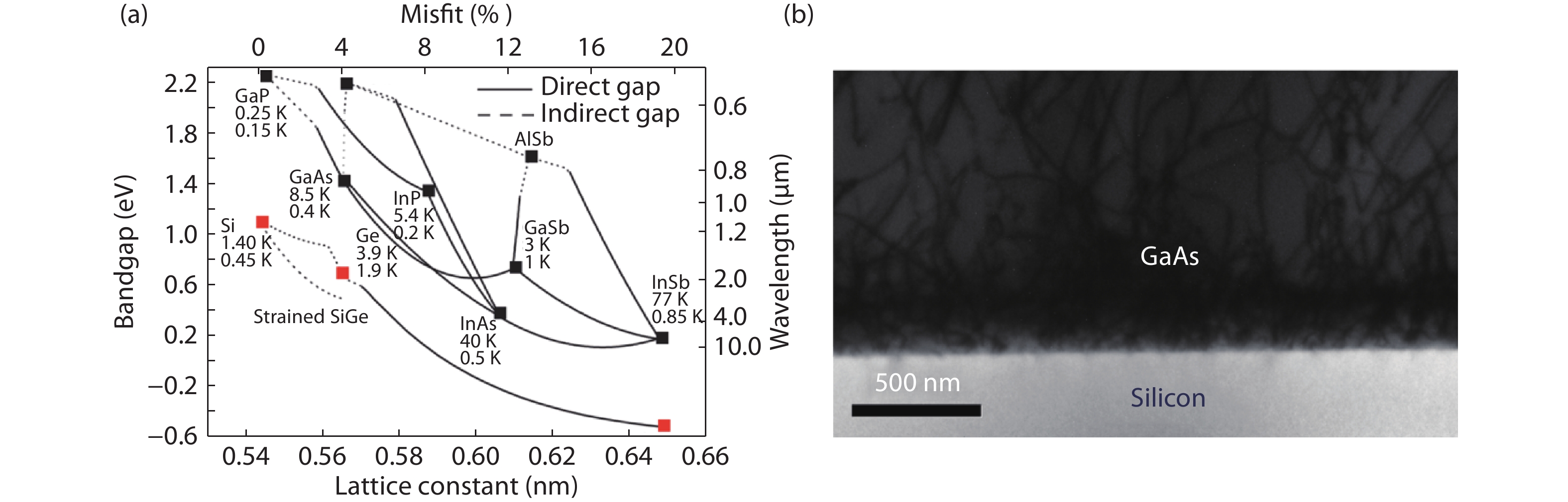
As shown in Fig. 1(a), the existence of approximately 4% (7.5%) lattice mismatch between GaAs (InP) and Si[
![]()
Figure 1.(Color online) (a) The plot of bandgap energy and wavelength versus lattice constant and misfit between III–V and group IV [
As mentioned above, when the III–V materials with polar bonds are grown on non-polar group IV substrates, due to the existence of monoatomic steps on the group IV substrates, the antiphase boundaries (APBs) occur[
![]()
Figure 2.(Color online) (a) Schematic showing polar/nonpolar interface between GaAs and Ge. Mono-atomic steps on Ge surface result in APBs, planes of As–As or Ga–Ga bonds. The antiphase domains (APBs) can also self-annihilate (left) or rise to the epi-layer surface (right). Diatomic steps on the Ge surface (center) do not result in APB formation[
Due to the different thermal expansion coefficients between III–V and group IV materials (Si: 2.59 × 10⁻⁶ K–1, GaAs: 5.73 × 10⁻⁶ K–1), the thermal stress will accumulate in the thick III–V epi-layer when the wafer is cooled down from high growth temperature to room temperature, which will lead to formation of thermal micro-cracks (see Fig. 3) to relieve the thermal stress. The thickness of III–V epi-layer and the change of wafers’ temperature (ΔT) both have an important influence on the formation of thermal micro-cracks. Critical thickness of the crack formation on GaAs epi-layer on Si to be experimentally observed is approximately 7 μm for a ΔT of 575 °C, 5.1 μm for a ΔT of 675 °C, and 4.9 μm for a ΔT of 725 °C[
![]()
Figure 3.Optical microscope image of the thermal cracks on III–V/Si surface.
2. Hetero-epitaxial growth of III–V QDs on Ge and (111)-faceted Si (001) substrates
As stated above, to realize the low-cost, high-yield, reliable and epitaxially grown Si-based III–V QD laser for Si photonics integration, the three major obstacles must be overcome. The progress of highly efficient O-band and C/L-band wavelength emission of InAs QDs on both Ge and Si substrates[
2.1. InAs QDs on Ge substrates
The first InAs QD laser with ultra-high performance on Ge substrate was reported in the year of 2011 by Liu et al.[
Comparing to the work reported previously[
![]()
Figure 4.(Color online) (a) 5 × 5
Based on the high quality and ultra-flat GaAs layer on Ge substrate, a standard O-band structure with five-layer InAs/GaAs dot-in-a-well (DWELL) was grown at 450 °C. It is identical to those optimized structures grown on GaAs substrate. The schematic of the structure is shown in Fig. 5(a). Here, each DWELL layer consists of a 6-nm In0.14Ga0.86As capping layer, a 3.1-monolayer (ML) InAs QD layer and a 2-nm In0.14Ga0.86As wetting layer. The capping layer and wetting layer were grown at 450 °C. The 50 nm GaAs spacer layers were grown at an optimum temperature of 560 °C between each InAs/GaAs DWELLs. The room-temperature (RT) PL spectra were shown in Fig. 5(b), which indicate similar PL intensity can be obtained on both GaAs/Ge substrate and GaAs substrate. High quality five-layer DWELL structure with defect free can be obtained, with a dot density of 3.6 × 1010 cm–2, as shown in the zoomed-in TEM image in the inset.
![]()
Figure 5.(Color online) (a) The schematic of 5-layer InAs/GaAs QD structure grown on Ge substrate for O-band wavelength emission. (b) RT PL spectra of InAs/GaAs QDs on GaAs/Ge substrate and GaAs substrate, respectively. Inset: Zoomed-in cross-sectional TEM image of InAs/GaAs QDs on GaAs/Ge substrate.
Since most of passive and active devices for Si photonics are based on C-band long-haul telecommunications, III–V light sources on Si at 1.55 μm are becoming strongly demanded. It is believed that the Si-based high-gain III–V semiconductor optical amplifiers (SOAs) at C/L-band are essential components for the long-haul transmission[
For the growth of InGaAs metamorphic buffer layer on GaAs/Ge substrate, step-graded epitaxial growth method and cycle annealing process were both conducted to get high-quality InGaAs layers. First, a step-graded InGaAs layer of the thickness of 200 nm from In0.09Ga0.91As to In0.13Ga0.87As was deposited on GaAs/Ge substrate, followed by a 200 nm In0.13Ga0.87As layer, which were both grown at 380 °C. Then, another step-graded InGaAs layer from In0.13Ga0.87As to In0.25Ga0.75As was deposited at 380 °C, followed by a 100 nm In0.25Ga0.75As layer grown at 500 °C. To further reduce the defect density, the wafer was annealed at 500 °C for 30 min adjacently after each growth of InGaAs buffer layer of 200 nm thick. As the 5 × 5 μm2 AFM image shows in Fig. 6(a), a flat In0.25Ga0.75As metamorphic buffer layer was achieved on GaAs/Ge substrate with a 0.45 nm RMS.
![]()
Figure 6.(Color online) (a) 5 × 5
The active region consisting of 3 periods of InAs QD layer was grown on the flat top and high quality In0.25Ga0.75As buffer layer. Each InAs QD layer was made up of 2.8-ML InAs capped by a 4 nm In0.25Ga0.75As, which were both grown at 465 °C. The 45 nm In0.25Ga0.75As spacer layers used to separate the InAs QD layers were grown at an optimized temperature of 500 °C. Cross-sectional TEM characterization of the whole structure was conducted, and it is presented in Fig. 6(b). Fig. 6(c) shows the high-magnification TEM image of a truncated InAs/InGaAs QD. Moreover, PL measurements of InAs/InGaAs QDs on both Ge and GaAs substrates were characterized, and normalized RT PL spectra are shown in Fig. 6(d). The PL intensity of InAs/InGaAs QDs on Ge substrates at C/L-band wavelength is about 85% of that on GaAs substrates. The 1 × 1 μm2 AFM image of InAs QDs on Ge substrate is shown in the inset of Fig. 6(d), with a dot density of 2.55 × 1010 cm–2. More details can be found in Ref. [41].
2.2. InAs QD monolithically grown on (111)-faceted Si (001) substrates
Although many works on 1300 nm InAs QD lasers have been reported on offcut Ge and Si substrates[
U-shaped pattern with ridges along [110] direction on standard 8-inch Si (001) wafers were prepared as following: 1) SiO2 deposition as hard mask, 2) U-shape pattern by deep ultraviolet (DUV) photolithography, 3) dry etching, and 4) removal of SiO2 in a diluted hydrofluoric acid (HF) solution. As shown in Fig. 7(a), a period of 360 nm with a 140 nm width ridge and a 500 nm depth groove in the U-shape pattern is achieved following the process described above. 3.2 × 3.2 cm2 dies can be obtained by cleaving this 8-inch wafer. After ex-situ chemical cleaning, and oxide layer removal in a diluted HF solution, the patterned Si substrate was loaded into SiGe MBE chamber and heated up to 720 °C for outgassing. Then homoepitaxy of 550 nm Si layer was conducted at a growth rate of 1.0 Å/s at 600 °C. After that, the (111)-faceted Si hollow structures were achieved on the U-shape patterned Si (001) substrate, as shown in Fig. 7(b). The Si substrate with hollow structures was then transferred to the III–V MBE chamber for the following hybrid growth. Fig. 7(c) shows the SEM image of III–V buffer layer on (111)-faceted Si hollow substrate. Owing to the novel (111)-faceted structures, the APBs and dislocation defects can be confined at the III–V/Si (111) interface. More importantly, the thermal stress during the temperature change of substrates can benefit from this hollow structure.
![]()
Figure 7.(Color online) (a), (b) and (c) Cross-sectional SEM images of U-shape patterned Si substrate, homoepitaxy of 550 nm Si on (111)-faceted Si hollow substrate, and III–V buffer layers on (111)-faceted Si hollow substrate, respectively. All the images are taken along the [110] axis. (d) 10 × 10
The GaAs buffer layers were deposited by using a two-step method consisting of a 40-nm-thick buffer layer grown at 380 °C and a 560-nm-thick buffer layer grown at 580 °C. To note, before the main GaAs layers, a 10-nm-thick AlAs layer was deposited on the (111) facets as a nucleation layer at a growth rate of 0.5 Å/s, which can significantly reduce the defect density at the III–V/Si interface due to the higher bonding energy of AlAs[
The cross-sectional TEM, electron channeling contrast imaging (ECCI), and plan-view TEM measurements were carried out to verify the quality of GaAs layers on Si (001). Cross-sectional TEM image taken along [110] axis of GaAs on (111)-faceted Si hollow substrate is presented in Fig. 8(a). It shows that most of the defects are confined at the III–V/Si interface. In addtion, the defects propagate into the upper region lying on (111) planes, and they will merge at the tip of sawtooth structures and then annihilate. This is due to the high symmetry and uniformity of homoepitaxially formed Si sawtooth structures. InGaAs/GaAs DFLs could then completely filter some propagating dislocations. Moreover, the EECI and plan-view TEM results shown in Fig. 8(b) and Fig. 8(c) show that a low defect density (ECCI: 4.8 × 106 cm–2, and plan-view TEM: 7.0 × 106 cm–2) was observed on the surface of GaAs/Si (001). By means of these specially designed Si (001) substrates and hybrid epitaxy method, high-quality and smooth GaAs layers can be achieved on on-axis Si (001) substrate, which serves as an essential platform for integration of III–V photonic structures on Si (001) substrates.
![]()
Figure 8.(Color online) (a) Cross-sectional TEM image of GaAs on (111)-faceted Si hollow substrate, taken along [110] axis. (b) Plan-view ECCI to show TDs on GaAs/Si template. (c) Plan-view TEM image of GaAs surface on Si.
On the high-quality GaAs/Si (001) platforms, the 1300 and 1550 nm InAs QD structures are grown, respectively. The standard five-layer InAs/GaAs DWELL structure was grown on GaAs/Si (001) substrate for the 1300 nm wavelength emission. The material growth details can be found in section 2.1. More importantly, although there is some work about lasers on Si with C/L-band telecom window emission[
The PL measurements at room temperature of InAs/GaAs and InAs/InGaAs QDs on both GaAs substrates and GaAs/Si substrates were carried out, and PL spectra at O-band and C/L-band are both shown in Fig. 9. Fig. 9(a) shows typical PL emission at 1300 nm with a FWHM of 36 meV from InAs/GaAs QDs on GaAs/Si (001) substrates. It is suggested that the stronger peak intensity in PL spectrum on Si substrate may result from the enhanced pump power from bottom grating-like (111)-faceted Si structures[
![]()
Figure 9.(Color online) (a) RT PL spectra of InAs/GaAs QDs grown on both GaAs and GaAs/Si (001) substrates, for O-band emission. Inset: 1 × 1
In summary, highly efficient O-band and C/L-band emission of InAs QDs monolithically grown on CMOS-compatible Si (001) substrates have been achieved by using (111)-faceted Si (001) hollow structures via a dual-chamber in-situ hybrid growth method. More importantly, the (111)-faceted Si (001) hollow structures can release the thermal stress between III–V epitaxial layers and Si substrate in a certain extent. This growth method enables the possibility of fabricating high yield and performance III–V optoelectronic devices covering the two communication windows (1300 and 1550 nm) on CMOS-compatible Si (001) substrates.
3. Optically pumped 1300 nm InAs QD micro-disk lasers on (111)-faceted Si (001) susbtrates
Due to the advantages of high quality-factor, small footprint, and low power consumption[
We have demonstrated the high-quality GaAs layers on (111)-faceted Si (001) hollow substrate without defects, APBs, and thermal cracks. The microdisk laser structures were grown on these GaAs/Si (001) platforms, which consisted of a 600 nm Al0.7Ga0.3As sacrificial layer and a 700 nm disk region. The active region consists of a 7-layer InAs DWELLs, and the DWELL structure was grown at the same condition as described in section 2.1. At last, 50 nm thick Al0.4Ga0.6As layer was deposited to enclose the active region as a barrier. Moreover, a reference sample on standard GaAs substrate was grown with identical growth conditions for comparison purpose. Fig 10(a) shows the schematic diagram of the whole microdisk laser structure. For the fabrication of microdisk lasers, the 4 μm-diameter silica beads acted as the hard mask for the standard inductive coupled plasma (ICP) etching, followed by subsequent wet etching process. After removal of silicon beads, the microdisk lasers were achieved with a diameter of 4 μm. Fig. 10(b) shows the schematic diagram of a microdisk laser. Figs. 10(c) and 10(d) present the tilted SEM images of microdisk lasers on GaAs (001) and GaAs/Si (001) substrates, respectively. Both disk structures show vertical profile, smooth sidewall. The microdisk lasers on GaAs and Si (001) substrates are both characterized in the following part.
![]()
Figure 10.(Color online) Schematic diagrams of (a) microdisk laser structure and (b) microdisk laser on GaAs/Si (001) substrate. (c) and (d) Tilted SEM images of microdisk lasers on GaAs (001) and GaAs/Si (001) substrates, respectively.
The microdisk lasers on GaAs and Si (001) substrate were measured under a micro-PL system with 532 nm-continuous-wave semiconductor laser. Figs. 11(a) and 11(c) show the integrated intensity of microdisk lasers versus the pump power (L–L curve) on GaAs substrate and Si (001) substrate, respectively. The laser on Si (001) substrate has a pump power threshold as low as 380 μW, which is almost the same as that (330 μW) of the lasers on GaAs substrate. Typical ‘S-shaped’ nonlinear transition are shown both clearly in the insets of Figs. 11(a) and 11(c), including all three regimes of opeartion: spontaneous emission, amplified spontaneous emission and laser oscillation[
![]()
Figure 11.(Color online) Integrated intensity of microdisk lasers versus the power of pump laser on (a) GaAs substrate and (c) Si (001) substrate, respectively. Inset: the log–log plot of ‘L–L curve’. PL spectra of microdisk lasers on (b) GaAs substrate and (d) Si (001) substrate, respectively, under different pump powers.
Figs. 11(b) and 11(d) show the lasers’ spectra of the devices on GaAs and Si (001) substrate under different pump power. From the spectra, a high cavity quality factor (Q) of 3674 is obtained for the InAs QD lasers on Si (001) substrate, which is a little larger than that (3550) on GaAs substrate. Here, the higher Q-factor of microdisk on Si (001) substrate might result from the underneath grating-like Si patterns. The spacing of 17 and 18 nm between the adjacent modes in the same radial-order on GaAs substrate and Si (001) substrate, are obtained, respectively, agreeing well with the calculation result. In conclusion, high-performance O-band InAs QD microdisk lasers are achieved on CMOS-compatible Si (001) substrates, which show great pontetial as a light source in the integration of optoelectronic devices.
4. Summary and outlook
In conclusion, we have reported recent progress of hybrid epitaxially grown InAs QD microcavity lasers on (111)-faceted Si (001) substrates. A novel (111)-faceted Si (001) hollow substrate was invented to obtain defect-free, APB-free, and thermal crack-free III–V photonic structures on Si (001) platforms. High-efficient O-band and C/L band emission of InAs QDs were achieved on Si (001) substrates. In addition, high-performance O-band microdisk lasers were realized and characterized on the (111)-faceted Si (001) hollow substrates. Here, this hybrid epitaxial growth technique will provide a promising approach to migrate III–V optoelectronic materials on Si platforms for the future silicon photonics integration.
Acknowledgments
The financial support was provided by the National Natural Science Foundation of China (Nos. 61635011, 11574356, 11434010, 61804177 and 11804382); National Key Research and Development Program of China (Nos. 2016YFA0300600 and 2016YFA0301700); Key Research Program of Frontier Sciences, CAS (No. QYZDB-SSW-JSC009); Ting Wang was supported by the Youth Innovation Promotion Association of CAS (No. 2018011).
References
[1] M Asghari, A V Krishnamoorthy. Silicon photonics: Energy-efficient communication. Nat Photonics, 5, 268(2011).
[2] A Rickman. The commercialization of silicon photonics. Nat Photonics, 8, 579(2014).
[3] A Vahdat, H Liu, X Zhao et al. The emerging optical data center. Optical Fiber Communication Conference, OTuH2(2011).
[4] J F Bauters, M L Davenport, M J R Heck et al. Silicon on ultra-low-loss waveguide photonic integration platform. Opt Express, 21, 544(2013).
[5] M J R Heck, J F Bauters, M L Davenport et al. Ultra-low loss waveguide platform and its integration with silicon photonics. Laser Photonics Rev, 8, 667(2014).
[6] T Yin, R Cohen, M M Morse et al. 31 GHz Ge n–i–p waveguide photodetectors on silicon-on-insulator substrate. Opt Express, 15, 13965(2007).
[7] L Vivien, A Polzer, D Marris-Morini et al. Zero-bias 40 Gbit/s germanium waveguide photodetector on silicon. Opt Express, 20, 1096(2012).
[8] G T Reed, G Mashanovich, F Y Gardes et al. Silicon optical modulators. Nat Photonics, 4, 518(2010).
[9] X Xiao, H Xu, X Li et al. High-speed, low-loss silicon Mach-Zehnder modulators with doping optimization. Opt Express, 21, 4116(2013).
[10] X Zheng, I Shubin, G Li et al. A tunable 1 × 4 silicon CMOS photonic wavelength multiplexer/demultiplexer for dense optical interconnects. Opt Express, 18, 5151(2010).
[11] D Liang, J E Bowers. Recent progress in lasers on silicon. Nat Photonics, 4, 511(2010).
[12] H Rong, A Liu, R Jones et al. An all-silicon Raman laser. Nature, 433, 292(2005).
[13] R E Camacho-Aguilera, Y Cai, N Patel et al. An electrically pumped germanium laser. Opt Express, 20, 11316(2012).
[14] J Liu, X Sun, D Pan et al. Tensile-strained, n-type Ge as a gain medium for monolithic laser integration on Si. Opt Express, 15, 11272-11277(2007).
[15] A Y Liu, J Bowers. Photonic integration with epitaxial III–V on silicon. IEEE J Sel Top in Quantum Electron, 24, 1(2018).
[16] K Tanabe, K Watanabe, Y Arakawa. III–V/Si hybrid photonic devices by direct fusion bonding. Sci Rep, 2, 349(2012).
[17] Z Wang, K Van Gasse, V Moskalenko et al. A III–V-on-Si ultra-dense comb laser. Light: Sci Appl, 6, e16260(2017).
[18] Z Zhou, B Yin, J Michel. On-chip light sources for silicon photonics. Light: Sci Appl, 4, e358(2015).
[19] Z Wang, A Abbasi, U Dave et al. Novel light source integration approaches for silicon photonics. Laser Photonics Rev, 11, 1700063(2017).
[20] C W Liu, M Östling, J B Hannon. New materials for post-Si computing. MRS Bulletin, 39, 658(2014).
[21] J Wu, S Chen, A Seeds et al. Quantum dot optoelectronic devices: lasers, photodetectors and solar cells. J Phys D, 48, 363001(2015).
[22] M Tang, S Chen, J Wu et al. 1.3-
[23] J Wang, H Y Hu, C Deng et al. Defect reduction in GaAs/Si film with InAs quantum-dot dislocation filter grown by metalorganic chemical vapor deposition. Chin Phys B, 24, 028101(2015).
[24] Q Li, K M Lau. Epitaxial growth of highly mismatched III–V materials on (001) silicon for electronics and optoelectronics. Prog Cryst Growth Charact Mater, 63, 105(2017).
[25] J Faucher, T Masuda, M L Lee. Initiation strategies for simultaneous control of antiphase domains and stacking faults in GaAs solar cells on Ge. J Vac Sci Technol B, 34, 041203(2016).
[26] M Liao, S Chen, J S Park et al. III–V quantum-dot lasers monolithically grown on silicon. Semicond Sci Technol, 33, 123002(2018).
[27] G Brammertz, Y Mols, S Degroote et al. Low-temperature photoluminescence study of thin epitaxial GaAs films on Ge substrates. J Appl Phys, 99, 093514(2006).
[28] R Alcotte, M Martin, J Moeyaert et al. Epitaxial growth of antiphase boundary free GaAs layer on 300 mm Si (001) substrate by metalorganic chemical vapour deposition with high mobility. Appl Mater, 4, 046101(2016).
[29] M Akiyama, Y Kawarada, K Kaminishi. Growth of single domain GaAs layer on (100)-oriented Si substrate by MOCVD. Jpn J Appl Phys, 23, L843(1984).
[30] D J Chadi. Stabilities of single-layer and bilayer steps on Si (001) surfaces. Phys Rev Lett, 59, 1691(1987).
[31] T Wang, H Liu, A Lee et al. 1.3-
[32] A Lee, Q Jiang, M Tang et al. Continuous-wave InAs/GaAs quantum-dot laser diodes monolithically grown on Si substrate with low threshold current densities. Opt Express, 20, 22181(2012).
[33] M Liao, S Chen, S Huo et al. Monolithically integrated electrically pumped continuous-wave III–V quantum dot light sources on silicon. IEEE J Sel Top Quantum Electron, 23, 1(2017).
[34] S Chen, M Liao, M Tang et al. Electrically pumped continuous-wave 1.3
[35] J Norman, M J Kennedy, J Selvidge et al. Electrically pumped continuous wave quantum dot lasers epitaxially grown on patterned, on-axis (001) Si. Opt Express, 25, 3927(2017).
[36] K Volz, A Beyer, W Witte et al. GaP-nucleation on exact Si (001) substrates for III/V device integration. J Cryst Growth, 315, 37(2011).
[37] A Y Liu, J Peters, X Huang et al. Electrically pumped continuous-wave 1.3
[38] D Jung, Z Zhang, J Norman et al. Highly reliable low-threshold InAs quantum dot lasers on on-axis (001) Si with 87% injection efficiency. ACS Photonics, 5, 1094(2017).
[39] J Kwoen, B Jang, J Lee et al. All MBE grown InAs/GaAs quantum dot lasers on on-axis Si (001). Opt Express, 26, 11568(2018).
[40] V K Yang, M Groenert, C W Leitz et al. Crack formation in GaAs heteroepitaxial films on Si and SiGe virtual substrates. J Appl Phys, 93, 3859(2003).
[41] W Q Wei, J H Wang, Y Gong et al. C/L-band emission of InAs QDs monolithically grown on Ge substrate. Opt Mater Express, 7, 2955(2017).
[42] W Q Wei, J H Wang, B Zhang et al. InAs QDs on (111)-faceted Si (001) hollow substrates with strong emission at 1300 nm and 1550 nm. Appl Phys Lett, 113, 053107(2018).
[43] Q Feng, W Wei, B Zhang et al. O-band and C/L-band III–V quantum dot lasers monolithically grown on Ge and Si substrate. Appl Sci, 9, 385(2019).
[44] H Liu, T Wang, Q Jiang et al. Long-wavelength InAs/GaAs quantum-dot laser diode monolithically grown on Ge substrate. Nat Photonics, 5, 416(2011).
[45] P Kaspar, R Brenot, A Le Liepvre et al. Packaged hybrid III–V/silicon SOA. The European Conference on Optical Communication (ECOC), 1(2014).
[46] N N Ledentsov, A R Kovsh, A E Zhukov et al. High performance quantum dot lasers on GaAs substrates operating in 1.5
[47] T Wang, A Lee, F Tutu et al. The effect of growth temperature of GaAs nucleation layer on InAs/GaAs quantum dots monolithically grown on Ge substrates. Appl Phys Lett, 100, 052113(2012).
[48] A Lee, H Liu, A Seeds. Semiconductor III–V lasers monolithically grown on Si substrates. Semicond Sci Technol, 28, 015027(2012).
[49] A D Lee, Q Jiang, M Tang et al. InAs/GaAs quantum-dot lasers monolithically grown on Si, Ge, and Ge-on-Si substrates. IEEE J Sel Top Quantum Electron, 19, 1901107(2013).
[50] A Y Liu, C Zhang, J Norman et al. High performance continuous wave 1.3
[51] S Chen, W Li, J Wu et al. Electrically pumped continuous-wave III–V quantum dot lasers on silicon. Nat Photonics, 10, 307(2016).
[52] Y Wan, Q Li, Y Geng et al. InAs/GaAs quantum dots on GaAs-on-V-grooved-Si substrate with high optical quality in the 1.3
[53] Y Wan, Q Li, A Y Liu et al. Temperature characteristics of epitaxially grown InAs quantum dot micro-disk lasers on silicon for on-chip light sources. Appl Phys Lett, 109, 011104(2016).
[54] Q Li, K W Ng, K M Lau. Growing antiphase-domain-free GaAs thin films out of highly ordered planar nanowire arrays on exact (001) silicon. Appl Phys Lett, 106, 072105(2015).
[55] B Shi, S Zhu, Q Li et al. Continuous-wave optically pumped 1.55
[56] B Shi, S Zhu, Q Li et al. 1.55
[57] S Zhu, B Shi, Y Wan et al. 1.55
[58] Y Wan, D Jung, C Shang et al. Low-threshold continuous-wave operation of electrically pumped 1.55
[59] B Zhang, W Q Wei, J H Wang et al. 1310 nm InAs quantum-dot microdisk lasers on SOI by hybrid epitaxy. Opt Express, 27, 19348(2019).
[60] S L McCall, A F J Levi, R E Slusher et al. Whispering-gallery mode microdisk lasers. Appl Phys Lett, 60, 289(1992).
[61] Y Wan, Q Li, A Y Liu et al. Optically pumped 1.3
[62] Q Li, Y Wan, A Y Liu et al. 1.3-
[63] Y Wan, J Norman, Q Li et al. 1.3
[64]

Set citation alerts for the article
Please enter your email address
© Copyright 2018-2021 | Chinese Laser Press. All Rights Reserved 沪ICP备15018463号-20