• Journal of Semiconductors
  • Vol. 43, Issue 9, 092802 (2022)
Qian Jiang1、2, Junhua Meng3, Yiming Shi1、3, Zhigang Yin1、4, Jingren Chen1、4, Jing Zhang2、*, Jinliang Wu1, and Xingwang Zhang1、4、**
Author Affiliations
  • 1Key Lab of Semiconductor Materials Science, Institute of Semiconductors, Chinese Academy of Sciences, Beijing 100083, China
  • 2School of Information Science and Technology, North China University of Technology, Beijing 100144, China
  • 3Faculty of Science, Beijing University of Technology, Beijing 100124, China
  • 4Center of Materials Science and Optoelectronics Engineering, University of Chinese Academy of Sciences, Beijing 100049, China
  • show less
    DOI: 10.1088/1674-4926/43/9/092802 Cite this Article
    Qian Jiang, Junhua Meng, Yiming Shi, Zhigang Yin, Jingren Chen, Jing Zhang, Jinliang Wu, Xingwang Zhang. Electrical and optical properties of hydrogen plasma treatedβ-Ga2O3 thin films[J]. Journal of Semiconductors, 2022, 43(9): 092802 Copy Citation Text show less
    (Color online) (a) XRDθ–2θ pattern of theβ-Ga2O3 thin films grown onc-plane sapphire substrates. The inset shows the XRD rocking curve of theβ-Ga2O3 (2¯01) reflection. (b) In-plane XRD Phi scans of for theβ-Ga2O3 film and sapphire substrate. (c) Cross-sectional HRTEM image of theβ-Ga2O3 film on sapphire. (d) XPS core-level spectra of O 1s and Ga 2p.
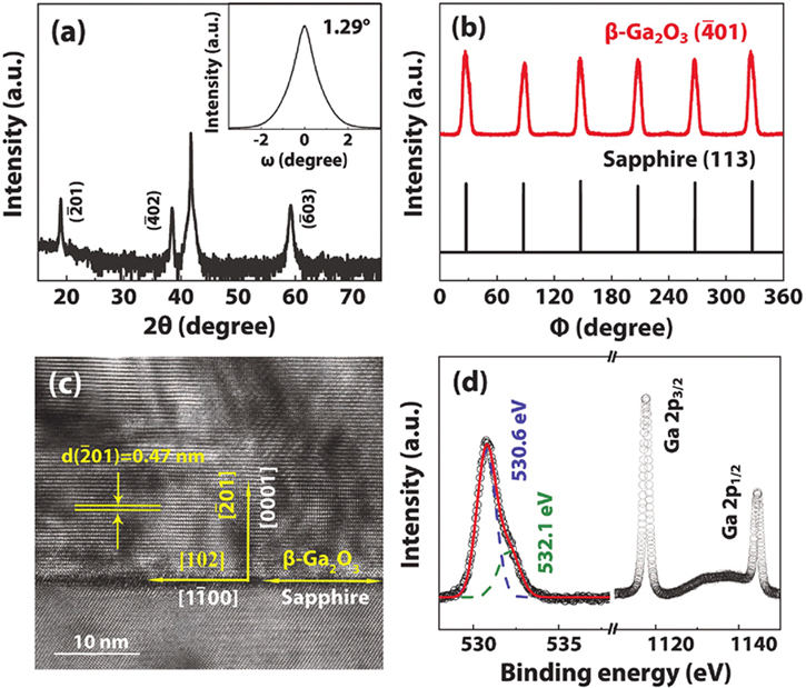
    Fig. 1. (Color online) (a) XRDθ–2θ pattern of theβ-Ga2O3 thin films grown onc-plane sapphire substrates. The inset shows the XRD rocking curve of theβ-Ga2O3 ( 2¯01) reflection. (b) In-plane XRD Phi scans of for theβ-Ga2O3 film and sapphire substrate. (c) Cross-sectional HRTEM image of theβ-Ga2O3 film on sapphire. (d) XPS core-level spectra of O 1s and Ga 2p.
    (Color online) (a) SIMS depth profiles of the H-plasma treatedβ-Ga2O3 film on sapphire substrate. (b) Raman spectra of theβ-Ga2O3 film with and without H-plasma treatment. (c) XRDθ–2θ pattern of theβ-Ga2O3 thin films with and without the H-plasma treatment. (d) XRD rocking curve of theβ-Ga2O3 (2¯01) reflection for theβ-Ga2O3 film with and without the H-plasma treatment. (e) UV–vis absorption spectra of theβ-Ga2O3 film with and without H-plasma treatment. The Tauc plots of (αhν)2 versushν is shown in the inset. (f) PL spectra of theβ-Ga2O3 film with and without H-plasma treatment. The H-plasma treatment was carried out with an RF power of 40 W and a H2 flow rate of 50 sccm for 120 min.
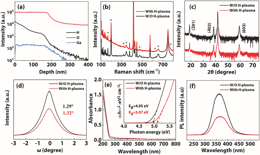
    Fig. 2. (Color online) (a) SIMS depth profiles of the H-plasma treatedβ-Ga2O3 film on sapphire substrate. (b) Raman spectra of theβ-Ga2O3 film with and without H-plasma treatment. (c) XRDθ–2θ pattern of theβ-Ga2O3 thin films with and without the H-plasma treatment. (d) XRD rocking curve of theβ-Ga2O3 ( 2¯01) reflection for theβ-Ga2O3 film with and without the H-plasma treatment. (e) UV–vis absorption spectra of theβ-Ga2O3 film with and without H-plasma treatment. The Tauc plots of (αhν)2 versus is shown in the inset. (f) PL spectra of theβ-Ga2O3 film with and without H-plasma treatment. The H-plasma treatment was carried out with an RF power of 40 W and a H2 flow rate of 50 sccm for 120 min.
    (Color online) Dependence of (a) the resistivity and (b) the Hall data of theβ-Ga2O3 films on the H-plasma exposure time. Dependence of (c) the resistivity and (d) the Hall data of theβ-Ga2O3 films on the RF power. Dependence of (e) the resistivity and (f) the Hall data of theβ-Ga2O3 films on the H2 flow rate.
    Fig. 3. (Color online) Dependence of (a) the resistivity and (b) the Hall data of theβ-Ga2O3 films on the H-plasma exposure time. Dependence of (c) the resistivity and (d) the Hall data of theβ-Ga2O3 films on the RF power. Dependence of (e) the resistivity and (f) the Hall data of theβ-Ga2O3 films on the H2 flow rate.
    (Color online) Temperature dependent (a) carrier concentration, (b) electron mobility, and (c) electrical resistivity for two typicalβ-Ga2O3 thin films after the H-plasma treatment. Dashed lines show the contributions to mobility from different scattering mechanisms, and the solid line shows the fitting total mobility.
    Fig. 4. (Color online) Temperature dependent (a) carrier concentration, (b) electron mobility, and (c) electrical resistivity for two typicalβ-Ga2O3 thin films after the H-plasma treatment. Dashed lines show the contributions to mobility from different scattering mechanisms, and the solid line shows the fitting total mobility.
    Qian Jiang, Junhua Meng, Yiming Shi, Zhigang Yin, Jingren Chen, Jing Zhang, Jinliang Wu, Xingwang Zhang. Electrical and optical properties of hydrogen plasma treatedβ-Ga2O3 thin films[J]. Journal of Semiconductors, 2022, 43(9): 092802
    Download Citation