Abstract
The behavior of H inβ-Ga2O3 is of substantial interest because it is a common residual impurity that is present inβ-Ga2O3, regardless of the synthesis methods. Herein, we report the influences of H-plasma exposure on the electric and optical properties of the heteroepitaxialβ-Ga2O3 thin films grown on sapphire substrates by chemical vapor deposition. The results indicate that the H incorporation leads to a significantly increased electrical conductivity, a greatly reduced defect-related photoluminescence emission, and a slightly enhanced transmittance, while it has little effect on the crystalline quality of theβ-Ga2O3 films. The significant changes in the electrical and optical properties ofβ-Ga2O3 may originate from the formation of shallow donor states and the passivation of the defects by the incorporated H. Temperature dependent electrical properties of the H-incorporatedβ-Ga2O3 films are also investigated, and the dominant scattering mechanisms at various temperatures are discussed.The behavior of H inβ-Ga2O3 is of substantial interest because it is a common residual impurity that is present inβ-Ga2O3, regardless of the synthesis methods. Herein, we report the influences of H-plasma exposure on the electric and optical properties of the heteroepitaxialβ-Ga2O3 thin films grown on sapphire substrates by chemical vapor deposition. The results indicate that the H incorporation leads to a significantly increased electrical conductivity, a greatly reduced defect-related photoluminescence emission, and a slightly enhanced transmittance, while it has little effect on the crystalline quality of theβ-Ga2O3 films. The significant changes in the electrical and optical properties ofβ-Ga2O3 may originate from the formation of shallow donor states and the passivation of the defects by the incorporated H. Temperature dependent electrical properties of the H-incorporatedβ-Ga2O3 films are also investigated, and the dominant scattering mechanisms at various temperatures are discussed.Introduction
Monoclinic structureβ-Ga2O3 is emerging as a promising semiconductor for next generation high power devices and solar-blind ultraviolet (UV) detectors, due to its ultra-wide bandgap (~4.9 eV), high breakdown electric field (~8 MV/cm), good chemical and thermal stability, as well as large area substrates grown by low-cost and scalable melt-growth methods[1-5]. The precise control of carrier type and concentration is a prerequisite for most device applications[6]. However, undopedβ-Ga2O3 usually exhibits strong n-type conductivity, which is unfavorable for p-type doping inβ-Ga2O3 because of a compensation effect. Oxygen vacancy (VO) and Ga interstitial (Gai) have been excluded as the causes of this background conductivity owing to their deep donor levels. Unintentionally incorporated H is also considered to be a possible factor leading to the n-type conductivity ofβ-Ga2O3. It has been reported that H can not only introduce a shallow donor[7-10] but can also form complexes with other extrinsic and intrinsic defects, which passivates their electrical activity[11,12]. The exact origin of this n-type background conductivity ofβ-Ga2O3 is not yet elucidated.
Hydrogen can be introduced intoβ-Ga2O3 via high temperature annealing in H2, H+ ion implantation and direct H-plasma exposure. Most experimental studies have been focused on the configuration of H-related defects by means of IR absorption spectra, capacitance–voltage profiling, and deep level transient spectroscopy[13-19]. An IR absorption peak at 3437 cm−1 was observed in the H-incorporatedβ-Ga2O3, assigned to the Ga vacancy (VGa) decorated with two H atoms (VGa-2H) defect complex[13]. Islamet al. reported that the VGa-2H complex leads to p-type behavior, while the trapping of four H atoms at Ga vacancy (VGa-4H) give rise to n-type conductivity[20]. Furthermore, Polyakovet al. reported that the electrical properties ofβ-Ga2O3 single crystals with a H-plasma treatment are highly anisotropic, depending on the surface crystal orientation[18]. The diffusion properties of H inβ-Ga2O3 at different temperatures have also been investigated from the concentration–depth profiles[21-23]. Although the configuration and dynamics of H-related defects have been widely studied, the systematic investigation on the influence of H-doping on electrical and optical properties is still insufficient. In particular, previous experimental studies were mainly carried out with bulkβ-Ga2O3 single crystal or homoepitaxialβ-Ga2O3 layer, and the H-doping of heteroepitaxialβ-Ga2O3 film has not yet been reported.
In this work, we report a systematic study on the effects of H-plasma treatment on the optical and electrical properties of heteroepitaxialβ-Ga2O3 thin films. It is found that the H-plasma treatedβ-Ga2O3 film exhibits n-type characteristics and enhanced conductivity, while its structure is not influenced by the H-plasma treatment. The enhanced electrical conductivity may be attributed to the shallow donor states resulting from the incorporated H. The dominant scattering mechanism is also discussed according to the temperature dependent electrical properties of the H-incorporatedβ-Ga2O3 films.
Experimental
The intrinsicβ-Ga2O3 thin films were deposited onc-plane sapphire substrates by low-pressure chemical vapor deposition (LPCVD), which has been depicted in our previous paper[24]. High purity Ga pellets and O2 were used as the precursors, and Ar with a flow rate of 50 sccm was used as the carrier gas. The Ga source and substrate temperatures were 840 and 800 °C, respectively. The growth time was 15 min and the thicknesses ofβ-Ga2O3 films were about 200 nm. To introduce H, the as-grownβ-Ga2O3 films were directly exposed to a capacitively coupled RF H-plasma at room temperature. The flow rate of pure H2 varied from 30 to 70 sccm, while the exposure time was changed from 10 to 180 min. The working pressure was kept at 50 Pa during plasma treatment, while the RF power varied from 10 to 110 W.
The microstructures of theβ-Ga2O3 films were characterized by transmission electron microscopy (TEM) by a FEI Talos F200X microscope and X-ray diffraction (XRD). XRD measurements were carried out by a Rigaku D/MAX-2500 system using Cu Kα as the x-ray source. X-ray photoelectron spectroscopy (XPS) were performed on a Thermo Scientific ESCALAB 250Xi spectrometer with a 1486.6 eV Al Kα radiation source. The H distribution in depth was obtained by a time-of-flight secondary ion mass spectrometry (ToF-SIMS) ToF-SIMS 5-100 system using a 2 keV Cs+ ion beam with an incidence angle of 45°. Raman spectroscopy was obtained with a confocal spectrometer using a 532 nm laser as the excitation source. The UV–vis absorption spectra were acquired with a Varian Cary 5000 UV–vis spectrophotometer. Photoluminescence (PL) spectra were measured at 10 K using a homemade DUV laser spectroscopy system with a 213 nm laser as the excitation source. The carrier concentration and mobility of theβ-Ga2O3 films were determined by an M91 FastHall measurement system (Lake Shore) using the Van der Pauw configuration.
Results and discussion
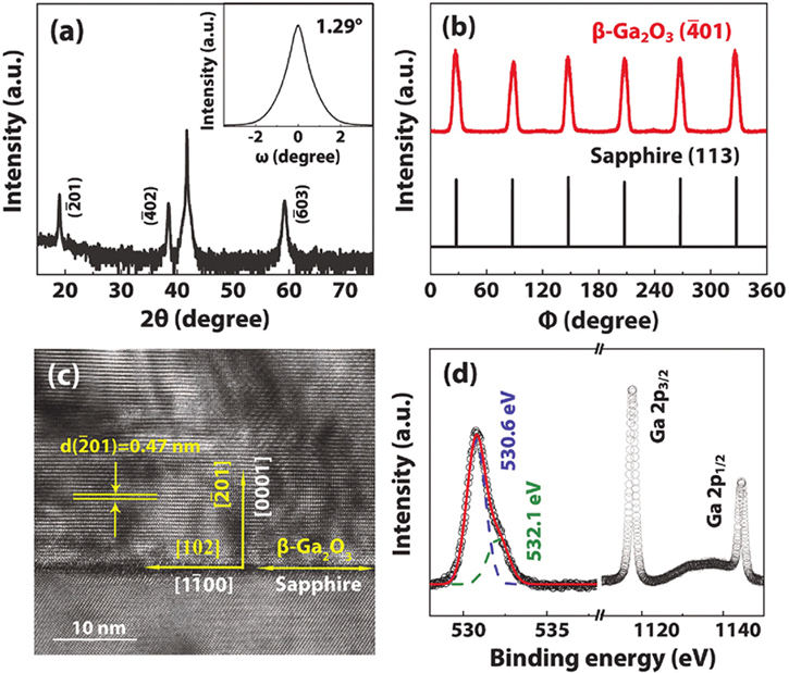
Fig. 1(a) shows a typical XRD pattern of theβ-Ga2O3 thin film on the sapphire substrate. Besides the diffraction peak from sapphire substrate, three diffraction peaks at 18.95°, 38.70°, and 59.20° are observed, which are indexed as the (
), (
), and (
) reflections ofβ-Ga2O3. The rocking curve of theβ-Ga2O3 (
) reflection is shown in the inset, showing a full width at half maximum (FWHM) of 1.29°, which is comparable with the reported values for theβ-Ga2O3 films on sapphire[25,26]. To extract the in-plane orientation betweenβ-Ga2O3 and sapphire, the XRD azimuthal scans were taken on theβ-Ga2O3 (
) and sapphire (113) reflections, respectively. As show inFig. 1(b), six diffraction peaks at 60° intervals are clearly observed for both Phi-scans at the same azimuthal angles, revealing an excellent in-plane orientation between them. These XRD results reveal that their epitaxial relationship isβ-Ga2O3 (
)//sapphire (006) andβ-Ga2O3 [102]//sapphire [
]. To observe the interface structure in atomic scale, a cross-sectional high-resolution TEM (HRTEM) image was taken along the [
] direction ofc-plane sapphire. The atomically sharp interface betweenβ-Ga2O3 and sapphire substrate is clearly resolved, indicating the high-quality epitaxial growth (Fig. 1(c)). The lattice fringes of 0.47 nm spacing are indexed to the (
) planes ofβ-Ga2O3, which matches well with the results of XRD.Fig. 1(d) shows the XPS spectra of the Ga 2p and O 1s core-levels for theβ-Ga2O3 film. The two distinct peaks at binding energies of 1117.1 and 1144.3 eV are assigned to the Ga 2p3/2 and Ga 2p1/2 core levels of the Ga-O bond, respectively[9,27]. The deconvolution of O 1s spectrum gives two peaks centered at 530.6 and 532.1 eV. The main peak at 530.6 eV is contributed to the Ga-O bond, while the shoulder peak at 532.1 eV originates from the adsorbed C–O or O–H species on the film surface[9,17,27].

Figure 1.(Color online) (a) XRDθ–2θ pattern of theβ-Ga2O3 thin films grown onc-plane sapphire substrates. The inset shows the XRD rocking curve of theβ-Ga2O3 (
) reflection. (b) In-plane XRD Phi scans of for theβ-Ga2O3 film and sapphire substrate. (c) Cross-sectional HRTEM image of theβ-Ga2O3 film on sapphire. (d) XPS core-level spectra of O 1s and Ga 2p.
SIMS measurement was performed to investigate the depth profile of H in theβ-Ga2O3 film. As shown inFig. 2(a), after the H-plasma treatment, H diffuses into the entireβ-Ga2O3 film with a gradually decreasing concentration with depth. The obtained H-profile is in good agreement with the diffusion behavior from a constant or semi-infinite source[28]. Similar depth profiles of H were also observed for the H-plasma treated ZnO andβ-Ga2O3[19,29,30], where depths of ~1µm were reported. In this work, the film thickness is about 200 nm; hence, H can diffuse into the wholeβ-Ga2O3 film. The nature of H migration inβ-Ga2O3 was identified to be monatomic H diffusion rather than molecular diffusion[22]. However, the configuration of H-related defects in the lattice is still ambiguous and under investigation.
Figure 2.(Color online) (a) SIMS depth profiles of the H-plasma treatedβ-Ga2O3 film on sapphire substrate. (b) Raman spectra of theβ-Ga2O3 film with and without H-plasma treatment. (c) XRDθ–2θ pattern of theβ-Ga2O3 thin films with and without the H-plasma treatment. (d) XRD rocking curve of theβ-Ga2O3 (
) reflection for theβ-Ga2O3 film with and without the H-plasma treatment. (e) UV–vis absorption spectra of theβ-Ga2O3 film with and without H-plasma treatment. The Tauc plots of (αhν)2 versushν is shown in the inset. (f) PL spectra of theβ-Ga2O3 film with and without H-plasma treatment. The H-plasma treatment was carried out with an RF power of 40 W and a H2 flow rate of 50 sccm for 120 min.
To clarify the effect of H-plasma treatment on the structure of theβ-Ga2O3 films, Raman and XRD measurements were performed with and without the H-plasma treatment. As shown inFig. 2(b), besides the Raman modes from the sapphire substrate, eight Raman peaks ofβ-Ga2O3 can be observed for both samples. The low frequency modes are ascribed to the vibration and translation of tetrahedra-octahedra chains, while the mid- and high-frequency modes are related to the vibration of Ga2O6 octahedra and GaO4 tetrahedra, respectively[31]. It should be noted that no new Raman peak is produced after the H-plasma exposure, and the FWHM values of the 199.6 cm−1 peak are rather close with and without the H-plasma treatment (3.4 and 3.5 cm−1). Similarly, the XRD patterns are almost not changed after the H-plasma treatment (Figs. 2(c) and2(d)). Obviously, the H-plasma treatment has little effect on the crystalline quality due to the relative “soft” treatment conditions in this work, which is one of the advantages of the plasma exposure over the ion implantation technique.
Fig. 2(e) shows the UV–vis absorption spectra of theβ-Ga2O3 films with and without plasma treatment. Both samples show a sharp absorption edge at ~250 nm, which is due to the optical bandgap, with an almost zero absorbance from 350 to 800 nm. The optical bandgapEg can be obtained from the Tauc relation of (αhν)2∝ (hν–Eg), whereα is the absorption coefficient andhν is the incident photon energy. As shown in the insert ofFig. 2(e), the bandgapEg slightly increases from 4.95 to 5.07 eV after the H-plasma exposure. The slight widening of the bandgap might be attributed to the Burstein-Moss effect because H-doping gives rise to a significant increase of electron concentration[32], which will be further confirmed by the Hall measurement later. A similar phenomenon has also been reported in other hydrogenated oxide semiconductors[33]. In addition, the transmittance in the 300–500 nm range increases after the H-plasma exposure, indicating the reduced sub-bandgap absorption from defects.
The PL spectra was measured to investigate the effect of H-doping on the optical properties ofβ-Ga2O3 films.Fig. 2(f) shows the low-temperature PL spectra of the intrinsic and the H-plasma treatedβ-Ga2O3 films. Both samples exhibit a broad UV luminescence (UVL) band at ~370 nm, and the lack of near band-edge emission is a common feature for the luminescence spectrum ofβ-Ga2O3 due to the presence of self-trapped holes (STHs)[34-36]. This broad UVL band may be related to the recombination of free electrons with STHs or the self-trapped excitons, as well as the transition from the deep donor level to the acceptor level inβ-Ga2O3[35]. The self-trapped excitons consist of electrons on donors that are formed by VO and holes on acceptors that are formed by VGa or VO–VGa vacancy pairs. Regardless of the exact luminescence mechanism, the deep acceptor VGa should be involved in the broad UVL band because it is easy to exist inβ-Ga2O3 due to its low formation energy[36]. The incorporation of H into theβ-Ga2O3 film leads to a significant decrease in the defect-related PL emission, which probably can be ascribed to the passivation of defects. For instance, it was reported that the VGa defects can be effectively passivated by forming VGa-nH complexes[37]. Similar observation on the passivation of the defect-related emission due to the H incorporation was also reported previously[33].
To explore electrical properties, the Hall measurement was performed for theβ-Ga2O3 films with and without plasma treatment. However, it fails for the intrinsicβ-Ga2O3 film due to its semi-insulating nature. After the H-plasma treatment, the resistivity of theβ-Ga2O3 films is significantly reduced to allow the Hall measurement, where metal indium pads were used as the contact electrodes, revealing a good ohmic contact. As expected, the H-incorporatedβ-Ga2O3 films exhibit n-type conductivity with the highest room-temperature mobility of 45 cm2/(V·s). The influences of H-plasma treatment on the electrical characteristics ofβ-Ga2O3 films have been systematically investigated, as shown inFig. 3. For each condition, four samples were measured and the error bars inFig. 3 represent the standard error of the measured data, showing an acceptable reproducibility. Theβ-Ga2O3 films were first exposed to an H-plasma with a fixed RF power of 40 W and a H2 flow rate of 50 sccm at room temperature with various exposure times from 10 to 180 min.Figs. 3(a) and3(b) present the dependence of the resistivity and the Hall data of theβ-Ga2O3 films on the H-plasma exposure time, respectively. As shown inFig. 3(a), the resistivity of theβ-Ga2O3 film gradually decreases with increasing exposure time, up to 150 min, and it remains steady thereafter. The mobility gradually increases from 27.6 to 41.8 cm2/(V·s) as the exposure time increases from 10 to 120 min, and then it slightly decreases for longer exposure times. The carrier concentration (4 × 1018 cm−3) does not show an obvious variation when the exposure time is below 120 min, and then increases to 5.8 × 1018 cm−3. Obviously, a 10-min H-plasma treatment is enough to obtain a high electron concentration of >1018 cm−3 and a moderate mobility, and the optimum treatment time is 120–150 min. The formation of the shallow donor level in theβ-Ga2O3 film by the incorporated H may be responsible for the great increase of carrier concentration. The interstitial Hi has a low formation energy under both Ga-rich and O-rich conditions, and thus it is easily incorporated as an unintentional donor impurity[7]. The increasing mobility means that the incorporated H can also passivate defects and/or acceptor impurities, possibly by forming the VGa-nH complexes, which is consistent with the PL results.
Figure 3.(Color online) Dependence of (a) the resistivity and (b) the Hall data of theβ-Ga2O3 films on the H-plasma exposure time. Dependence of (c) the resistivity and (d) the Hall data of theβ-Ga2O3 films on the RF power. Dependence of (e) the resistivity and (f) the Hall data of theβ-Ga2O3 films on the H2 flow rate.
The dependences of the resistivity and the Hall data of theβ-Ga2O3 films on the RF power are shown inFigs. 3(c) and3(d), respectively. It is found that the carrier concentration rapidly decreases when the RF power exceeds 60 W, while the mobility gradually increases with increasing RF power up to 80 W and then slightly decreases. As a result, the resistivity of the H-treatedβ-Ga2O3 film remains unchanged when the RF power is less than 60 W, and it then increases with further increasing RF power. In the case of RF power being higher than 60 W, the decreasing carrier concentration and mobility may be attributed to the formation of different H-related defects. The interstitial Hi and H substituting at an O site (HO) can act as shallow donors, but the VGa-nH complexes exhibit donor or acceptor behavior depending on the number of H atoms in the vacancy[20]. Herein, the dependence of electrical properties ofβ-Ga2O3 films on the RF power may be related to the various configurations of H-related defects formed under different RF powers.
The effects of the H2 flow rate on the electrical properties ofβ-Ga2O3 films were also studied when the H-plasma exposure time and the RF power were kept at 120 min and 40 W, respectively. As shown inFig. 3(e), the resistivity shows a minimum value of ~27 mΩ·cm at H2 flow rates of 50–60 sccm. Correspondingly, the carrier concentration and mobility show the same tendency and have respective peaks at H2 flow rates of 50–60 sccm (Fig. 3(f)). We propose that the configurations of H-related defects are associated with the plasmas conditions, which strongly depend on the H2 flow rate. Nevertheless, further study is required to reveal the exact configurations of H-related defects in theβ-Ga2O3 films.
To better understand the electrical conduction mechanism of the H-incorporatedβ-Ga2O3 films, temperature-dependent Hall measurements were carried out for two representative samples with the same treatment parameters. As shown inFig. 4(a), the carrier concentration shows a negligible increase with temperature. It was reported that the Hi inβ-Ga2O3 behaves as a shallow donor with a low activation energy of 15 meV[10], and the ε(+/–) level is even located about 0.2 eV deep within the conduction band when the Hi is captured by lone O pairs[7,17]. Such a low activation energy means that nearly all of the donors are completely ionized throughout the temperature range studied, thus the carrier concentration is almost invariant with temperature. In contrast, the mobility slightly decreases with increasing temperature, as shown inFig. 4(b). The mobility of semiconductor is usually limited by various scattering mechanisms, including ionized impurities or defects, lattice vibration (phonons) and grain boundary, roughness and so on. The temperature dependent mechanisms for the longitudinal optical (LO) phonon (µLO) and the ionized impurities (µi) can be expressed as:
, and
. In addition, the mobility limited by short range scattering from defects, roughness and grain boundary are all temperature independent or weakly dependent mechanisms, and it is defined asµ0. The total electron mobilityµ can be described using Matthiessen’s rule as 1/µ = 1/µ0 + 1/µLO + 1/µi. As shown inFig. 4(b), fitting of the measured mobility to the total mobilityµ shows a good agreement within the whole temperature range. Obviously, the temperature independent scattering is a dominant mechanism at temperature range 100–250 K, while the room temperature mobility ofβ-Ga2O3 is determined by the LO mode scattering. Moreover, the variation in mobility is larger than the variation in carrier concentration. Consequently, the resistivity slightly increases with increasing temperature for both samples, as shown inFig. 4(c).
Figure 4.(Color online) Temperature dependent (a) carrier concentration, (b) electron mobility, and (c) electrical resistivity for two typicalβ-Ga2O3 thin films after the H-plasma treatment. Dashed lines show the contributions to mobility from different scattering mechanisms, and the solid line shows the fitting total mobility.
Conclusions
In summary, we demonstrate the influences of H-plasma exposure on the electrical and optical properties of heteroepitaxialβ-Ga2O3 films. The incorporation of H into the entireβ-Ga2O3 film leads to significantly increased conductivity, a greatly reduced defect-related PL emission, and a slightly enhanced transmittance, while the crystalline quality remains unchanged. The formation of shallow donor states, such as Hi, may be responsible for the enhanced conductivity, and the incorporated H inβ-Ga2O3 may also passivate defects and/or acceptor impurities by forming complexes. The effects of H incorporation are very complicated and further study is required to reveal the exact configurations of H-related defects in theβ-Ga2O3 films. The carrier concentration is almost invariant throughout the temperature range of 80−300 K, which is due to the complete ionization of the H-related donor. The optical phonon scattering is the dominant mechanism limiting mobility at room temperature for the H-incorporatedβ-Ga2O3 films.
Acknowledgements
This work was supported by the National Natural Science Foundation of China (Grant Nos. 62174009, 61904174 and 61874106), the Natural Science Foundation of Beijing Municipality (Grant No. 4212045) and the Strategic Priority Research Program of Chinese Academy of Sciences (Grant No. XDB43000000).
References
[1] M Higashiwaki, K Sasaki, H Murakami et al. Recent progress in Ga2O3 power devices. Semicond Sci Technol, 31, 034001(2016).
[2] S J Pearton, J Yang, IV P H Cary et al. A review of Ga2O3 materials, processing, and devices. Appl Phys Rev, 5, 011301(2018).
[3] H W Xue, Q M He, G Z Jian et al. An overview of the ultrawide bandgap Ga2O3 semiconductor-based Schottky barrier diode for power electronics, application. Nanoscale Res Lett, 13, 290(2018).
[4] X H Chen, F F Ren, S L Gu et al. Review of gallium-oxide-based solar-blind ultraviolet photodetectors. Photo Res, 7, 381(2019).
[5] D Guo, Q Guo, Z Chen et al. Review of Ga2O3 based optoelectronic devices. Mater Today Phys, 11, 100157(2019).
[6] R Sharma, M E Law, F Ren et al. Diffusion of dopants and impurities inβ-Ga2O3. J Vac Sci Technol A, 39, 060801(2021).
[7] J B Varley, J R Weber, A Janotti et al. Oxygen vacancies and donor impurities inβ-Ga2O3. Appl Phys Lett, 97, 142106(2010).
[8] J B Varley, H Peelaers, A Janotti et al. Hydrogenated cation vacancies in semiconducting oxides. J Phys Condens Matter, 23, 334212(2011).
[9] T T Huynh, E Chikoidze, C P Irvine et al. Red luminescence in H-dopedβ-Ga2O3. Phy Rev Mater, 4, 085201(2020).
[10] P D C King, I McKenzie, T D Veal. Observation of shallow-donor muonium in Ga2O3: Evidence for hydrogen-induced conductivity. Appl Phys Lett, 96, 062110(2010).
[11] W B Fowler, M Stavola, Y Qin et al. Trapping of multiple H atoms at the Ga(1) vacancy inβ-Ga2O3. Appl Phys Lett, 117, 142101(2020).
[12] Y Qin, M Stavola, W B Fowler et al. Hydrogen centers inβ-Ga2O3: Infrared spectroscopy and density functional theory. ECS J Solid State Sci Technol, 8, Q3103(2019).
[13] P Weiser, M Stavola, W B Fowler et al. Structure and vibrational properties of the dominant O-H center inβ-Ga2O3. Appl Phys Lett, 112, 232104(2018).
[14] J R Ritter, J Huso, P T Dickens et al. Compensation and hydrogen passivation of magnesium acceptors inβ-Ga2O3. Appl Phys Lett, 113, 052101(2018).
[15] M E Ingebrigtsen, A Y Kuznetsov, B G Svensson et al. Impact of proton irradiation on conductivity and deep level defects inβ-Ga2O3. APL Mater, 7, 022510(2019).
[16] A Y Polyakov, I H Lee, N B Smirnov et al. Hydrogen plasma treatment ofβ-Ga2O3: Changes in electrical properties and deep trap spectra. Appl Phys Lett, 115, 032101(2019).
[17] J E N Swallow, J B Varley, L A H Jones et al. Transition from electron accumulation to depletion atβ-Ga2O3 surfaces: The role of hydrogen and the charge neutrality level. APL Mater, 7, 022528(2019).
[18] A Y Polyakov, I H Lee, A Miakonkikh et al. Anisotropy of hydrogen plasma effects in bulk n-typeβ-Ga2O3. J Appl Phys, 127, 175702(2020).
[19] A Venzie, A Portoff, C Fares et al. OH-Si complex in hydrogenated n-typeβ-Ga2O3:Si. Appl Phys Lett, 119, 062109(2021).
[20] M M Islam, M O Liedke, D Winarski et al. Chemical manipulation of hydrogen induced high p-type and n-type conductivity in Ga2O3. Sci Rep, 10, 6134(2020).
[21] S Ahn, F Ren, E Patrick et al. Deuterium incorporation and diffusivity in plasma-exposed bulk Ga2O3. Appl Phys Lett, 109, 242108(2016).
[22] N H Nickel, K Gellert. Monatomic hydrogen diffusion in β-Ga2O3. Appl Phys Lett, 116, 242102(2020).
[23] V M Reinertsen, P M Weiser, Y K Frodason et al. Anisotropic and trap-limited diffusion of hydrogen/deuterium in monoclinic gallium oxide single crystals. Appl Phys Lett, 117, 232106(2020).
[24] Y J Jiao, Q Jiang, J H Meng et al. Growth and characteristics ofβ-Ga2O3 thin films on sapphire (0001) by low pressure chemical vapour deposition. Vacuum, 189, 110253(2021).
[25] S Rafique, L Han, A T Neal et al. Heteroepitaxy of N-typeβ-Ga2O3 thin films on sapphire substrate by low pressure chemical vapor deposition. Appl Phys Lett, 109, 132103(2016).
[26] C Wu, D Y Guo, L Y Zhang et al. Systematic investigation of the growth kinetics ofβ-Ga2O3 epilayer by plasma enhanced chemical vapor deposition. Appl Phys Lett, 116, 072102(2020).
[27] J Tao, H L Lu, Y Gu et al. Investigation of growth characteristics, compositions, and properties of atomic layer deposited amorphous Zn-doped Ga2O3 films. Appl Surf Sci, 476, 733(2019).
[28] Borg R J, Dienes G J. An introduction to solid state diffusion. Boston: Elsevier, 2012
[29] S Ahn, F Ren, E Patrick et al. Thermal stability of implanted or plasma exposed deuterium in single crystal Ga2O3. ECS J Solid State Sci, 6, Q3026(2017).
[30] J B You, X W Zhang, P F Cai et al. Enhancement of field emission of the ZnO film by the reduced work function and the increased conductivity via hydrogen plasma treatment. Appl Phys Lett, 94, 262105(2009).
[31] S Rafique, L Han, M J Tadjer et al. Homoepitaxial growth ofβ-Ga2O3 thin films by low pressure chemical vapor deposition. Appl Phys Lett, 108, 182105(2016).
[32] N Y Lee, K J Lee, C Lee et al. Determination of conduction band tail and Fermi energy of heavily Si-doped GaAs by room-temperature photoluminescence. J Appl Phys, 78, 3367(1995).
[33] P F Cai, J B You, X W Zhang et al. Enhancement of conductivity and transmittance of ZnO films by post hydrogen plasma treatment. J Appl Phys, 105, 083713(2009).
[34] K Shimamura, E G Víllora, T Ujiie et al. Excitation and photoluminescence of pure and Si-dopedβ-Ga2O3 single crystals. Appl Phys Lett, 92, 201914(2008).
[35] J B Varley, A Janotti, C Franchini et al. Role of self-trapping in luminescence and p-type conductivity of wide-band-gap oxides. Phys Rev B, 85, 081109(2012).
[36] Y K Frodason, K M Johansen, L Vines et al. Self-trapped hole and impurity-related broad luminescence inβ-Ga2O3. J Appl Phys, 127, 075701(2020).
[37] Y Wei, X Li, J Yang et al. Interaction between hydrogen and gallium vacancies inβ-Ga2O3. Sci Rep, 8, 10142(2018).