• Journal of Semiconductors
  • Vol. 43, Issue 9, 092803 (2022)
Minglong Zhang1、2, Masao Ikeda1、2、*, Siyi Huang1、2, Jianping Liu1、2、**, Jianjun Zhu2, Shuming Zhang1、2, and Hui Yang1、2
Author Affiliations
  • 1School of Nano-Tech and Nano-Bionics, University of Science and Technology of China, Hefei 230026, China
  • 2Suzhou Institute of Nano-Tech and Nano-Bionics, Chinese Academy of Sciences, Suzhou 215123, China
  • show less
    DOI: 10.1088/1674-4926/43/9/092803 Cite this Article
    Minglong Zhang, Masao Ikeda, Siyi Huang, Jianping Liu, Jianjun Zhu, Shuming Zhang, Hui Yang. Ni/Pd-based ohmic contacts to p-GaN through p-InGaN/p+-GaN contacting layers[J]. Journal of Semiconductors, 2022, 43(9): 092803 Copy Citation Text show less
    (Color online) Schematic illustration of the contact layer structure and c-TLM pattern used to measure contact resistance.
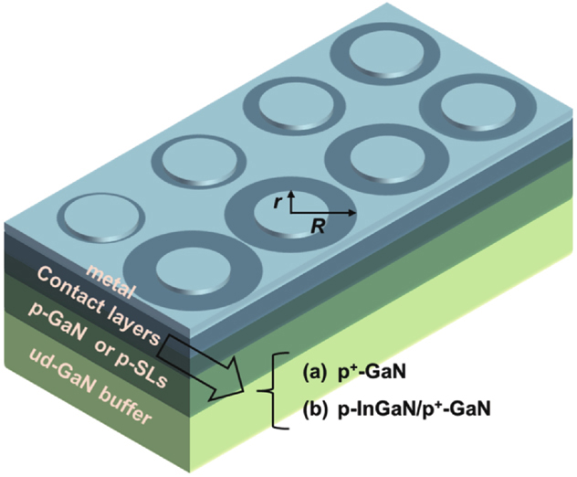
    Fig. 1. (Color online) Schematic illustration of the contact layer structure and c-TLM pattern used to measure contact resistance.
    (Color online) (a) The measured values of sheet resistance after annealing at various temperatures. (b) Comparison of the annealing temperature dependence ofρc between with and without the chemical surface treatment. (c, d) c-TLM-data examples for annealing temperature of 550 and 650 °C, respectively.
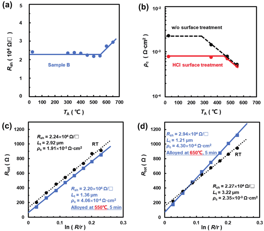
    Fig. 2. (Color online) (a) The measured values of sheet resistance after annealing at various temperatures. (b) Comparison of the annealing temperature dependence of ρc between with and without the chemical surface treatment. (c, d) c-TLM-data examples for annealing temperature of 550 and 650 °C, respectively.
    (Color online) Comparison ofTA-dependence ofρc between Ni 20 and Ni/Pd 2/60 contacts.
    Fig. 3. (Color online) Comparison ofTA-dependence of ρc between Ni 20 and Ni/Pd 2/60 contacts.
    (Color online) (a) Comparison ofρc–TA relation among three samples listed inTable 1. (b) Simulated valence band curves near the contact depletion region for the three samples.
    Fig. 4. (Color online) (a) Comparison of ρcTA relation among three samples listed inTable 1. (b) Simulated valence band curves near the contact depletion region for the three samples.
    (Color online) (a) STEM cross-sectional image of the sample C annealed at 550 °C. (b) EDX line analysis of Ga, In, Ni, Pd, Pt, and Au recorded along the blue arrow in Fig. 5(a).
    Fig. 5. (Color online) (a) STEM cross-sectional image of the sample C annealed at 550 °C. (b) EDX line analysis of Ga, In, Ni, Pd, Pt, and Au recorded along the blue arrow in Fig. 5(a).
    (Color online) The specific contact resistanceρc as a function of current density.
    Fig. 6. (Color online) The specific contact resistance ρc as a function of current density.
    Sampledp+-GaN (nm)[Mg]p+-GaN (1020 cm–3)dp-InGaN (nm)[Mg]p-InGaN (1019 cm–3)Xp-InGaN (%)Metal schemeSurface treatment
    A251Ni 20w/o
    B2013.587Ni 20w/o
    C2212420Ni/Pd 2/60w
    Table 1. Details of the structures of Ni/Pd-based metals and p-InGaN/p+-GaN contacting layers.
    Minglong Zhang, Masao Ikeda, Siyi Huang, Jianping Liu, Jianjun Zhu, Shuming Zhang, Hui Yang. Ni/Pd-based ohmic contacts to p-GaN through p-InGaN/p+-GaN contacting layers[J]. Journal of Semiconductors, 2022, 43(9): 092803
    Download Citation