Abstract
Specific contact resistance to p-GaN was measured for various structures of Ni/Pd-based metals and thin (20–30 nm thick) p-InGaN/p+-GaN contacting layers. The effects of surface chemical treatment and annealing temperature were examined. The optimal annealing temperature was determined to be 550 °C, above which the sheet resistance of the samples degraded considerably, suggesting that undesirable alloying had occurred. Pd-containing metal showed ~35% lower compared to that of single Ni. Very thin (2–3.5 nm thick) p-InGaN contacting layers grown on 20–25 nm thick p+-GaN layers exhibited one to two orders of magnitude smaller values of compared to that of p+-GaN without p-InGaN. The current density dependence of , which is indicative of nonlinearity in current-voltage relation, was also examined. The lowest achieved through this study was 4.9 × 10⁻⁵ Ω·cm2 @J = 3.4 kA/cm2.Specific contact resistance to p-GaN was measured for various structures of Ni/Pd-based metals and thin (20–30 nm thick) p-InGaN/p+-GaN contacting layers. The effects of surface chemical treatment and annealing temperature were examined. The optimal annealing temperature was determined to be 550 °C, above which the sheet resistance of the samples degraded considerably, suggesting that undesirable alloying had occurred. Pd-containing metal showed ~35% lower compared to that of single Ni. Very thin (2–3.5 nm thick) p-InGaN contacting layers grown on 20–25 nm thick p+-GaN layers exhibited one to two orders of magnitude smaller values of compared to that of p+-GaN without p-InGaN. The current density dependence of , which is indicative of nonlinearity in current-voltage relation, was also examined. The lowest achieved through this study was 4.9 × 10⁻⁵ Ω·cm2 @J = 3.4 kA/cm2.Introduction
GaN-based III-nitride is a wide bandgap material that has a wide range of applications in optoelectronics and power electronics, such as light emitting diodes(LEDs)[1], laser diodes (LDs)[2], and high electron mobility transistors (HEMTs)[3]. The p-GaN ohmic contact is an essential technology to improve the performance of GaN-based lasers. The operating current density of the laser is usually several kA/cm2. Under such high current injection, the device will seriously heat, which is detrimental to the lifetime and reliability of these devices. Therefore, the specific contact resistance should be desirably smaller than 10–4 Ω·cm2 to reduce the heat generation[4]. For the contact to n-GaN, specific contact resistivity on the order of 10–5–10–6 Ω·cm2 are easily obtained by applying Ti/Al, Ti/Au, or Ti/Al/Ni/Au metal schemes[5,6]. Compared to n-GaN, it is much more difficult to achieve low resistance ohmic contacts to p-GaN. The valence band of p-GaN is located at a quite deep level relative to the vacuum level, and it is generally much deeper than the Fermi levels of any metals. Therefore, metals with a large work function, such as Ni and Pd, are preferred for making ohmic contact to p-GaN. In addition, the activation energy of Mg in p-GaN is quite large ~160 meV[7], which makes it difficult to obtain a high hole concentration in p-GaN. Researchers have tried various methods to solve this problem, such as different metal schemes[8-11], alloying conditions[12,13], surface pretreatment[14-16], and so on. Kumakuraet al. formed ohmic contacts to p-GaN using strained InGaN contact layers, reporting as-deposited
as low as 10–6 Ω·cm2; however, they also reported thermal instability of the contacts; when the measurement temperature was elevated up to 400 °C, the value of
increased to a level of 10–4 Ω·cm2[17].
In this paper, Ni/Pd-based metals with p-InGaN/p+-GaN composite contacting layers exhibiting ohmic characteristics to p-GaN are reported. Compared to the contact layer structure of Kumakura et al., we inserted a heavily Mg-doped p+-GaN layer in between p-InGaN and p-GaN. The effect of surface treatment and annealing temperature were examined first. Low contact resistance can be obtained by optimizing the structures of contacting layers and the metal stacks. The current density dependence of the specific contact resistance is also reported.
Experiment methods
The p-GaN samples were grown on c-plane free-standing (FS-) GaN substrates using metal-organic chemical vapor deposition (MOCVD). Trimethy or triethyl gallium (TMGa/TEGa), ammonia (NH3), trimethylindium (TMIn), and bis-cyclopentadienyl magnesium (Cp2Mg) were used as the source materials for Ga, N, In, and Mg, respectively. A 1μm unintentionally doped GaN grown on FS-GaN substrate at 1000 °C, followed by 500 nm-thick Mg-doped p-GaN or 500 nm-thick p-AlGaN (2.5 nm)/p-GaN (2.5 nm) superlattice (SL) and 20–25 nm heavily Mg-doped p+-GaN were grown at 850 °C, finally, thin (2–3 nm) p-InGaN was grown at 740 °C. The Mg concentration in p-GaN and p-AlGaN/GaN SL were around 1 × 1019 cm–3, as evaluated by secondary ion mass spectroscopy (SIMS).
We used the circular transmission line model (c-TLM) to calculate the specific contact resistance
to characterize the ohmic properties of the contacts, and the total resistance between the two contacts is given by:
Table Infomation Is Not Enable
whereRsh is the sheet resistance of the p-GaN,Lt is the transfer length,r andR are the inner and outer radii of the circular pads in the c-TLM patterns.
Prior to metal deposition, the samples were annealed at 500 °C in a tube furnace in dry air to activate Mg by removing H from the p-type samples. This tube furnace was also used to anneal the contacts. The circular transmission line patterns were formed by standard photolithographic technique, with a contact inner radius (r) of 150μm and spacing (d) ranging from 5 to 40μm, respectively. Then, the metal films were deposited by an electron beam evaporation system (Ei-5z). Ni/Au (20 nm/200 nm) or Ni/Pd/Pt/Au (2 nm/60 nm/20 nm/200 nm) films were deposited under the pressure of 3.75 × 10⁻⁶ Torr. These two metal schemes are subsequently simplified as “Ni 20” and “Ni/Pd 2/60”, respectively. The electrical properties of contacts were measured by an Agilent B1500A semiconductor parametric analyzer employing a four-probe method. Scanning transmission electron microscopic (STEM) images combined with energy-dispersive X-ray spectroscopic (EDX) scans were used to analyze the metal/p-InGaN interfaces.
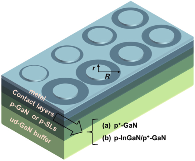
Fig. 1 shows the schematic of the sample structure and the c-TLM geometrical pattern. The ohmic characteristics for three structures listed inTable 1 were mainly compared.

Figure 1.(Color online) Schematic illustration of the contact layer structure and c-TLM pattern used to measure contact resistance.
Results and discussion
The effect of annealing temperature and chemical surface treatment were examined first using several wafers, having an identical contacting design to sample B (including different runs). The annealing temperature (TA) was varied between 300 and 650 °C, and the annealing time was fixed to 5 min.
As shown inFig. 2(a), the sheet resistance increases rapidly when the temperature exceeds 550 °C. From the c-TLM data at 550 and 650 °C inFigs. 2(c) and2(d), respectively, it can be seen more intuitively that although the specific contact resistance judged by the intercept of vertical axes is similar, the slope corresponding to the sheet resistance for the 650 °C line becomes much steeper than the as deposited slope. Meanwhile, the line of annealing temperature below 550 °C basically shifted downwards in parallel to the as deposited line, indicating only the reduction of the contact resistance while maintaining the sheet resistance. Although this phenomenon has not yet been fully understood, undesirable alloying into the p-GaN possibly occurred because the temperature was too high, which destroyed the thin InGaN layer and degraded the sheet resistance in the p-layer, or it might be related to the oxidization of the sample surface in the spacing region exposed to the air. Therefore, 550 °C can be determined as the optimum annealing temperature for the Ni 20 case, and the optimum annealing temperature for the Ni/Pd 2/60 nm case is also expected to be the same as for the Ni 20 nm case because the actual metal in contact directly with the semiconductor surface is both Ni metal in the two cases. Next, we checked the effect of chemical surface treatment. HCl+H2O (1 : 1) treatment just prior to the metal deposition makes the initial
level smaller by a factor of ~3, but at high annealing temperatures,
becomes eventually similar to those without surface treatment as shown inFig. 2(b). The surface treatment can only partly remove the contamination layer, and the annealing at the optimal temperature appears more effective in making better contacts between semiconductor and metal.
Figure 2.(Color online) (a) The measured values of sheet resistance after annealing at various temperatures. (b) Comparison of the annealing temperature dependence of
between with and without the chemical surface treatment. (c, d) c-TLM-data examples for annealing temperature of 550 and 650 °C, respectively.
In addition to the Ni/Au metal, Pd-based contacts were also examined. In our laboratory, Pd metal directly contacting to the InGaN surface often faced a serious problem of poor adhesion and peeling-off of the metal from the semiconductor surface easily happened. Consequently, making use of the good adhesive nature of Ni, a thin Ni was inserted between InGaN and Pd in order to help improve the adhesion property of the contacts. Samples having identical contacting layer design to sample B, without surface treatment were used to extract the difference between Ni 20 and Ni/Pd 2/60. The initial values of
were a little different among these samples within a factor of 1.7. Therefore, the data inFig. 3 were made by shifting the trend vertically along the
axis so that the initial levels align to the same level at 2 × 10⁻³ Ω·cm2 to make an exact comparison between different metals. As can be seen in the figure, the difference was not so large but the temperatureTc at which
starts to decrease and the decreasing rates are a little different for these two metal schemes. In the case of Ni 20,Tc is about 320 °C and the rate of decrease is × 0.54 per 100 °C, while for Ni/Pd 2/60,Tc is 305 °C, and the rate of decrease is × 0.44 per 100 °C increase. Eventually,
becomes ~35% lower for Pd-containing metal compared to that for single Ni at the optimum annealing temperature of 550 °C.
Figure 3.(Color online) Comparison ofTA-dependence of
between Ni 20 and Ni/Pd 2/60 contacts.
Fig. 4 (a) shows a comparison in
plotted against the annealing temperature for the three structures of different metals and p-InGaN/p+-GaN contacting layers as listed inTable 1. When comparing the
values, if the values of 550°C are taken, then the effect of surface treatment can be eliminated (as mentioned above). Then, the only contribution from the different metals must be taken into account. Consequently, the ratios of
for samples B and C relative to that of sample A becomes 0.17 and 0.028, respectively, if a 35% reduction of
from Ni/Au to Ni/Pd is taken into consideration. This indicates that the specific contact resistance of the p-InGaN/p+-GaN contacts can be lower by one to two orders of magnitude compared to the p+-GaN contact.
Figure 4.(Color online) (a) Comparison of
–TA relation among three samples listed inTable 1. (b) Simulated valence band curves near the contact depletion region for the three samples.
To understand these results qualitatively, the valence band curves around the depletion region near the contacting interface are simulated as shown inFig. 4(b). Since GaN has a large bandgap of 3.4 eV and an electron affinity of 4.1 eV, the depth of the valence band of p-GaN relative to the vacuum level amounts as large as 7.5 eV[18]. InFig. 4(b), the red solid line indicates the valence band of p-In0.2Ga0.8N (4 × 1019 cm–3)/p+-GaN (1 × 1020 cm–3) of sample C, the blue broken line is the valence band of p-In0.07Ga0.93N (8 × 1019 cm–3)/p+-GaN (1 × 1020 cm–3) of sample B, and the black line is that of p+-GaN (1 × 1020 cm–3) of sample A. In the case of the p-InGaN/p+-GaN contacting layer, the large band bending occurs due to the large piezoelectric polarization field together with the electric field due to the ionized acceptors in the interface depletion layer. However, the depletion layer of a single p+-GaN contact layer is mainly determined by the ionized impurity charge. Thus, according to our estimate shown in the figure, the effective width of the depletion region together with the barrier height becomes smaller in the order from A through B to C, which enhances the tunneling probability and consequently leads to a lower contact resistance. Here, the conduction-to-valence-band offset ratio of the GaN/InGaN interface was assumed as ΔEc : ΔEv = 60 : 40, and the polarization field in the In0.07Ga0.93N and In0.2Ga0.8N were assumed as 1.1 and 3.4 MV/cm[19], respectively. And the Fig. is drawn using the 5.2 eV work function of Pd.
The p-InGaN/p+-GaN contacting layer, of which InGaN had the same design as the best structure reported by Kumakuraet al.[17] coupled with the Ni/Pd 2/60 metal scheme, exhibited the lowest specific contact resistance of 4.9 × 10⁻⁵ Ω·cm2 in this study. Furthermore, this specific contact resistance should be thermally stable because the contact has already experienced a thermal annealing at 550 °C for 5 min.
Next, energy-dispersive X-ray spectroscopy (EDX) was performed for sample C annealed at 550 °C, to watch the extent of atomic inter diffusion. The STEM image is shown inFig. 5(a). The inset is an enlarged view of the black squared area, and it can be seen that the thickness of the InGaN layer is about 1.8 nm, which is consistent with the designed thickness of 2 nm, and the thin InGaN is confirmed to be surely remaining after the activation and annealing processes. Furthermore, no significant inter diffusion between metal and semiconductor (alloying) was observed in the EDX scans, as shown inFig. 5(b). Meanwhile, Pd metal is observed to have diffused through the thin Ni and have touched to the semiconductor surface. Thin Ni layer not only improves the adhesion of the contact but also allows Pd diffusing into the metal-semiconductor interface to make direct contact with p-InGaN, which improves the contact performance.
Figure 5.(Color online) (a) STEM cross-sectional image of the sample C annealed at 550 °C. (b) EDX line analysis of Ga, In, Ni, Pd, Pt, and Au recorded along the blue arrow in Fig. 5(a).
Finally, the dependence of
on the current density was also examined. When current-voltage characteristics are measured with a fixed voltage range, the current density flowing through each ring in the c-TLM becomes different because of the different contribution of sheet resistance (different gap length). Therefore, the current voltage characteristics were reexamined with fixed the current levels, under pulsed condition (pulse width: 500μs, pulse interval: 500 ms) to avoid the influence of heating effect. The results are shown inFig. 6. The obtained
did actually depend on the current density, which is indicative of some nonlinearity in the current-voltage relation as has been pointed out by Weimaret al.[20], even when the
level is very low. This means that, to be accurate, a
value must be stated with a measuring value of current density.
Figure 6.(Color online) The specific contact resistance
as a function of current density.
The lowest
obtained here correspond a value measured at 3.4 kA/cm2, which is close to the typical operating current density of LDs. Then, the voltage drop due to the contact resistance for a typical LD stripe with contact area of 1 × 10⁻⁴ cm2 can be estimated as
~ 0.12 V, which is small enough for practical use.
Conclusion
In summary, ohmic contacts formed using various structures of Ni/Pd-based metals and p-InGaN/p+-GaN contacting layers were studied. The surface treatment makes the initial
much smaller, but at a high annealing temperature
becomes similar to the untreated one. Compared with single Ni, Pd-containing metals exhibited better ohmic contact properties. By optimizing the annealing temperature and appropriately designing the contacting layers, the lowest
= 4.9 × 10⁻⁵ Ω·cm2 @J = 3.4 kA/cm2 could be obtained at 550 °C. The thin p-InGaN contacting layer was proven to be quite effective in realizing a good ohmic contact to p-GaN.
Acknowledgements
This work was funded by the National Key Research and Development Program of China (2017YFE0131500); the Key Research and Development Program of Guangdong Province (2020B090922001); National Natural Science Foundation of China (61834008); Key Research and Development Program of Jiangsu province (BE2020004, BE2021008-1); Guangdong Basic and Applied Basic Research Foundation (2019B1515120091). We are thankful for the technical support from Nano Fabrication Facility, Platform for Characterization & Test, and Nano-X of SINANO, CAS.
References
[1] S Nakamura. The roles of structural imperfections in InGaN-based blue light-emitting diodes and laser diodes. Science, 281, 956(1998).
[2] L Hu, X Y Ren, J P Liu et al. High-power hybrid GaN-based green laser diodes with ITO cladding layer. Photonics Res, 8, 279(2020).
[3] L Li, K Nomoto, M Pan et al. GaN HEMTs on Si with regrown contacts and cutoff/maximum oscillation frequencies of 250/204 GHz. IEEE Electron Device Lett, 41, 689(2020).
[4] Y Koide, T Maeda, T Kawakami et al. Effects of annealing in an oxygen ambient on electrical properties of ohmic contacts to p-type GaN. J Electron Mater, 28, 341(1999).
[5] B P Luther, S E Mohney, T N Jackson et al. Investigation of the mechanism for Ohmic contact formation in Al and Ti/Al contacts to n-type GaN. Appl Phys Lett, 70, 57(1997).
[6] K Singh, A Chauhan, M Mathew et al. Formation of non-alloyed Ti/Al/Ni/Au low-resistance ohmic contacts on reactively ion-etched n-type GaN by surface treatment for GaN light-emitting diodes applications. Appl Phys A, 125, 24(2019).
[7] T Tanaka, A Watanabe, H Amano et al. P-type conduction in Mg-doped GaN and Al0.08Ga0.92N grown by metalorganic vapor phase epitaxy. Appl Phys Lett, 65, 593(1994).
[8] J K Ho, C S Jong, C C Chiu et al. Low-resistance ohmic contacts to p-type GaN. Appl Phys Lett, 74, 1275(1999).
[9] J K Kim, J L Lee, J W Lee et al. Low resistance Pd/Au ohmic contacts to p-type GaN using surface treatment. Appl Phys Lett, 73, 2953(1998).
[10] S Wahid, N Chowdhury, M K Alam et al. Barrier heights and Fermi level pinning in metal contacts on p-type GaN. Appl Phys Lett, 116, 213506(2020).
[11] W J Wang, W Z Xie, Z J Deng et al. Performance improvement of GaN based laser diode using Pd/Ni/Au metallization ohmic contact. Coatings, 9, 291(2019).
[12] I Chary, A Chandolu, B Borisov et al. Influence of surface treatment and annealing temperature. J Electron Mater, 38, 545(2009).
[13] S P R Mallem, W H Ahn, J H Lee et al. Influence of thermal annealing on the PdAl/Au metal stack ohmic contacts to p-AlGaN. Crystals, 10, 1091(2020).
[14] J L Lee, M Weber, J K Kim et al. Ohmic contact formation mechanism of nonalloyed Pd contacts to p-type GaN observed by positron annihilation spectroscopy. Appl Phys Lett, 74, 2289(1999).
[15] J O Song, D S Leem, J S Kwak et al. High-quality nonalloyed rhodium-based ohmic contacts to p-type GaN. Appl Phys Lett, 83, 2372(2003).
[16] J L He, Y Z Zhong, Y Zhou et al. Recovery of p-GaN surface damage induced by dry etching for the formation of p-type Ohmic contact. Appl Phys Express, 12, 055507(2019).
[17] K Kumakura, T Makimoto, N Kobayashi. Ohmic contact to p-GaN using a strained InGaN contact layer and its thermal stability. Jpn J Appl Phys, 42, 2254(2003).
[18] J T Trexler, S J Pearton, P H Holloway et al. Comparison of Ni/Au, Pd/Au, and Cr/Au metallizations for ohmic contacts to p-GaN. MRS Online Proc Libr, 449, 1091(1996).
[19] F Bernardini, V Fiorentini. Spontaneous versus piezoelectric polarization in III-V nitrides: Conceptual aspects and practical consequences. Phys Status Solidi B, 216, 391(1999).
[20] A Weimar, A Lell, G Brüderl et al. Investigation of low-resistance metal contacts on p-type GaN using the linear and circular transmission line method. Phys Status Solidi A, 183, 169(2001).