- Journal of Semiconductors
- Vol. 43, Issue 9, 092803 (2022)
References
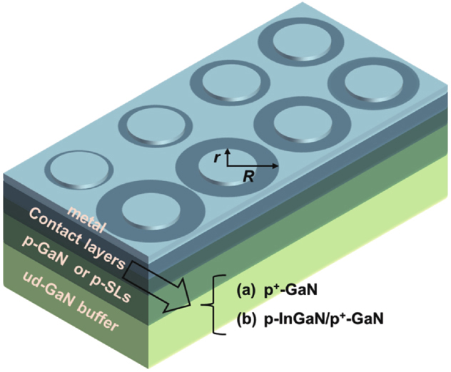

Minglong Zhang, Masao Ikeda, Siyi Huang, Jianping Liu, Jianjun Zhu, Shuming Zhang, Hui Yang. Ni/Pd-based ohmic contacts to p-GaN through p-InGaN/p+-GaN contacting layers[J]. Journal of Semiconductors, 2022, 43(9): 092803
Download Citation

Set citation alerts for the article
Please enter your email address
© Copyright 2018-2021 | Chinese Laser Press. All Rights Reserved 沪ICP备15018463号-20