• Acta Optica Sinica
  • Vol. 40, Issue 19, 1931001 (2020)
Shengquan He1, Haipeng Ke2、**, Lian Yan3, Xinglian Li1, Shaoying Ke1、*, and Dongke Li3
Author Affiliations
  • 1College of Physics and Information Engineering, Minnan Normal University, Zhangzhou, Fujian 363000, China
  • 2Zhangzhou First Vocational Secondary School, Zhangzhou, Fujian 363000, China
  • 3Huaiyin Normal University, Huaian, Jiangsu 223300, China
  • show less
    DOI: 10.3788/AOS202040.1931001 Cite this Article Set citation alerts
    Shengquan He, Haipeng Ke, Lian Yan, Xinglian Li, Shaoying Ke, Dongke Li. Effect of Interface State at Semiconductor-Insulator Contact Interface in Ge/Si Heterogeneous Bonding on Photoelectric Transport Characteristics of Heterojunction[J]. Acta Optica Sinica, 2020, 40(19): 1931001 Copy Citation Text show less
    Schematic of Ge/Si bonded heterojunction
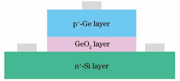
    Fig. 1. Schematic of Ge/Si bonded heterojunction
    Influence of ISD on dark current of Ge/Si heterojunction when T=300 K
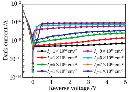
    Fig. 2. Influence of ISD on dark current of Ge/Si heterojunction when T=300 K
    Influence of ISD on total carrier recombination rate at different interfaces when T=300 K and bias voltage is -5 V. (a) Ge/GeO2 interface; (b) GeO2/Si interface
    Fig. 3. Influence of ISD on total carrier recombination rate at different interfaces when T=300 K and bias voltage is -5 V. (a) Ge/GeO2 interface; (b) GeO2/Si interface
    Influence of ISD on hole and electron concentrations in Ge and Si layers when T=300 K and bias voltage is -5 V. (a) Hole concentration; (b) electron concentration
    Fig. 4. Influence of ISD on hole and electron concentrations in Ge and Si layers when T=300 K and bias voltage is -5 V. (a) Hole concentration; (b) electron concentration
    Influence of ISD on electric filed and charge density when T=300 K and bias voltage is -5 V. (a) Electric fields in Ge and Si layers; (b) electric field in GeO2 layer; (c) charge density at Ge/Si interface
    Fig. 5. Influence of ISD on electric filed and charge density when T=300 K and bias voltage is -5 V. (a) Electric fields in Ge and Si layers; (b) electric field in GeO2 layer; (c) charge density at Ge/Si interface
    Influence of ISD on electron and hole speeds in Ge layer when T=300 K and bias voltage is -5 V. (a) Electron speed; (b) hole speed
    Fig. 6. Influence of ISD on electron and hole speeds in Ge layer when T=300 K and bias voltage is -5 V. (a) Electron speed; (b) hole speed
    Influence of ISD on total current and spectral response of Ge/Si heterojunction. (a) Total current; (b) spectral response
    Fig. 7. Influence of ISD on total current and spectral response of Ge/Si heterojunction. (a) Total current; (b) spectral response
    Influence of ISD on frequency response and 3 dB bandwidth of Ge/Si heterojunction when T=300 K and bias voltage is -5 V. (a) Frequency response ; (b) 3 dB bandwidth
    Fig. 8. Influence of ISD on frequency response and 3 dB bandwidth of Ge/Si heterojunction when T=300 K and bias voltage is -5 V. (a) Frequency response ; (b) 3 dB bandwidth
    Influence of bias voltage on Ge/Si heterojunction when T=300 K and ISD is 1×1010 cm-2. (a)Frequency response; (b) 3 dB bandwidth; (c) electric field
    Fig. 9. Influence of bias voltage on Ge/Si heterojunction when T=300 K and ISD is 1×1010 cm-2. (a)Frequency response; (b) 3 dB bandwidth; (c) electric field
    Influence of bias voltage on carrier speed when T=300 K and ISD is 1×1010 cm-2. (a) Electron speed in Ge layer; (b) electron speed in Si layer; (c) hole speed in Ge layer; (d) hole speed in Si layer
    Fig. 10. Influence of bias voltage on carrier speed when T=300 K and ISD is 1×1010 cm-2. (a) Electron speed in Ge layer; (b) electron speed in Si layer; (c) hole speed in Ge layer; (d) hole speed in Si layer
    Influence of ISD on electron tunneling rate at Ge/Si bonded interface when T=300 K and bias voltage is -5 V
    Fig. 11. Influence of ISD on electron tunneling rate at Ge/Si bonded interface when T=300 K and bias voltage is -5 V
    Shengquan He, Haipeng Ke, Lian Yan, Xinglian Li, Shaoying Ke, Dongke Li. Effect of Interface State at Semiconductor-Insulator Contact Interface in Ge/Si Heterogeneous Bonding on Photoelectric Transport Characteristics of Heterojunction[J]. Acta Optica Sinica, 2020, 40(19): 1931001
    Download Citation