
Jianqiu Hou, Zengwen Hu, Kuowen Lai, Yule Sun, Bo Shao, Chunyang Wang, Xinran Liu, Karson Liu. The investigation of DARC etch back in DRAM capacitor oxide mask opening[J]. Journal of Semiconductors, 2021, 42(7): 074101
- Journal of Semiconductors
- Vol. 42, Issue 7, 074101 (2021)
Abstract
1. Introduction
The dynamic random access memory (DRAM) industry has addressed an ongoing challenge to shrink the size of the device[
To form high-performance capacitors in the DRAM device, most research prefers to develop novel materials for high-dielectric layers[
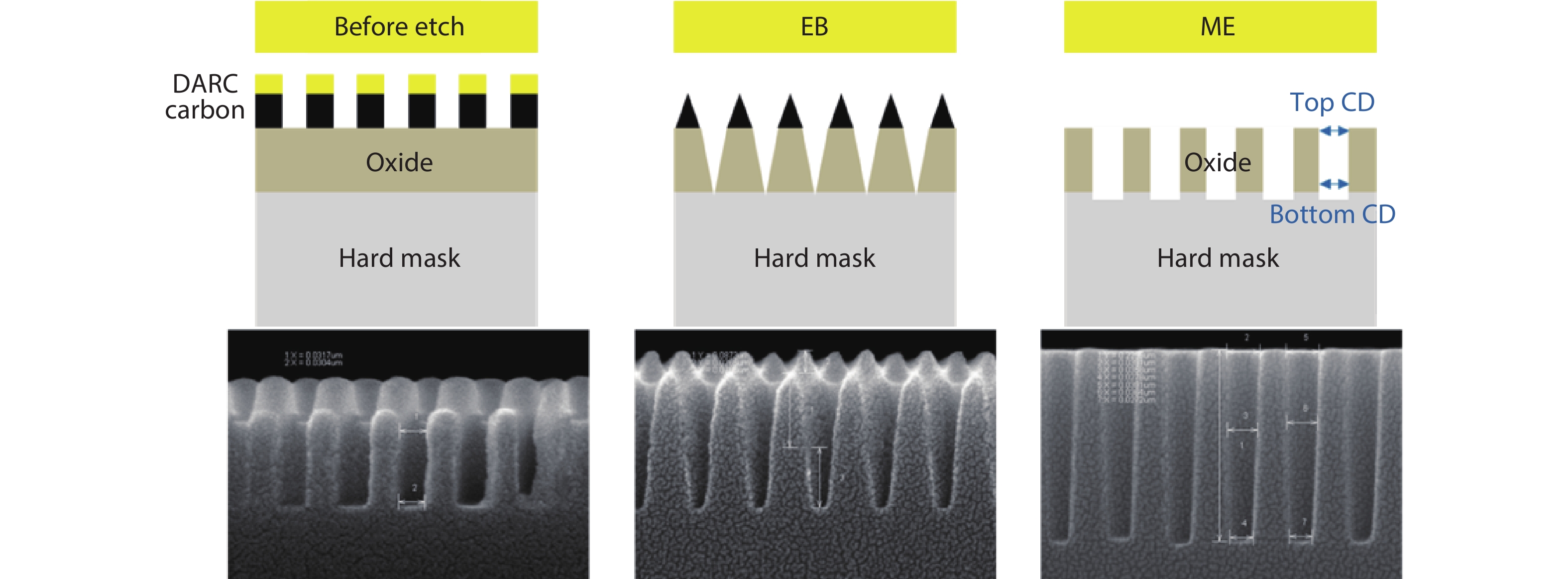
Therefore, we focus on studying and improving the oxide-mask-open process of the DRAM capacitor. The CD and profile of SiOx will influence the properties of the HM-Si mask (HM hard mask), further influencing the main etch of capacitor. The oxide mask process are consisting of three steps, DARC etch back (EB), SiOx main etch(ME), and stripping remained carbon.
The strategy and profile of SiOx mask open are shown in Fig. 1. The DARC layer is generally composed of Si O N for reducing the surface reflection, thus maximizing light collection efficiency in lithography. The carbon layer is set as a mask for following SiOx ME. DARC and carbon mask here have been already opened by “double-patterning” strategy. The purpose of etch back is to remove DARC on the top of the feature. Typically, due to the similar component of DARC and SiOx, the SiOx layer can also been etched to a taper profile in the EB step. Then we use ME step to full open the oxide layer and stop at the HM-Si layer. To obtain more straight holes i.e. high B/T ratio and baseline CD, we usually extend the time for over etch (OE). Finally, we should strip the remaining carbon to avoid some defect issues.
![]()
Figure 1.The strategy of etching oxide mask in the DRAM capacitor.
Here, we study DARC etch back due to the importance of beginning. Firstly, we found that DARC etch time can decide the profile of the oxide mask. It can be ascribed to the low selectivity of etching DARC and SiO2, based on traditional CF4/CHxFy/O2 chemistry. The profile of oxide mask thus become taper in DARC etch back step, which is reversed to our expectation. We would like to obtain a relative straight profile to the end. Thereby, we have to reduce the etch time and extend ME or OE time to obtain more straight holes i.e. high B/T ratio. However, not enough etch back time will result in DRAC remaining. It can lead to defect issues in the integration flow. According to the results, 50–60 s etch time is reasonable and appropriate. To evaluate the effect of DARC etch back on capacitor final CD, we also optimized the CH2F2 flow. We found that final CD is increased by 2.4% when CH2F2 increases from 15 to 25 sccm. It is an abnormal phenomenon because CH2F2 can produce amounts of a sticky CxFy polymer based on a free radical coupling mechanism. The polymer will be absorbed on hole side-wall and protect it from the physical bombarment as well as chemical reaction, indicating that higher flow of CH2F2 will usually result in smaller CD. However, in our case, too much CH2F2 will remain in some carbon polymers in the following HM-Si mask open process. It will consume some O2, which is a protective gas in Si etch, thereby leading to the larger final CD. The results indicate that we can control CH2F2 flow in DARC etch back step to change the final CD trend. Compared with the baseline process, our optimized process shows better profile, no DARC remaining and controlled final CD trend. All the results are from the co-work of equipment company and wafer fabrication company, suggesting the necessity and importance of further coporation in developing DRAM capacitors.
2. Experiment
All etching experiments were conducted in 300 mm capacitive coupled plasma (CCP) etch tool with two radio frequency (RF) frequency generator (50–60 MHz source and 2–3 MHz bias power). The etch tool is AMEC HD RIE. Typically, three steps were used to etch oxide masks in a DRAM capacitor: DARC etching back, silicon oxide (SiOx) main etch and remained carbon mask ashing. CF4/CHF3/CH2F2 chemistry were used to etch DARC (SiON) at etch back (EB) step. C4F6/C4F8/Ar/O2 chemistry were used to etch oxide (SiO2) at the main etch (ME) step. O2 chemistry were used to strip carbon at the strip step.
To avoid wasting resources, here we use “coupon”, a small chip sample cut from whole wafer, for experiment. The coupon has already been pre-coated with designed film stack and exposed for following etching process. We then paste the chip on a carrier wafer as a sample. To decrease the variation between the sample and whole wafer, we coat it with photoresist/SiO2 film stacks. The open ratio of the sample is similar with that of the whole wafer.
A 2 × 3 cm2 chip sample was pasted on a 300 mm carrier wafer to test in AMEC lab. The film stack of carrier wafer is photoresist/SiO2 from top to bottom. The open ratio of photoresist is about 50% with chess board pattern. 300 mm-structure whole wafers were used as samples in CXMT fab.
AMEC lab XSEM and top view metrology tool is Hitachi 4800 SEM. CXMT inline CD track tool is AMAT CDSEM.
3. Result and discussion
3.1. AMEC Lab chip test: Taper profile vs long EB time
To evaluate the effect of etch time step by step, we did 30 s partial etch in EB and ME step respectively. Fig. 2(a) shows that the etch depth, indicating the in-hole etch rate (ER) is 2.36 nm/s. Fig. 2(b) shows that the etch depth after 30 s ME, implying the in-hole ER is 4.76 nm/s. The ratio of in-hole ER between EB and ME step is around 1 : 2. Besides, the post-etch profiles of the oxide layer are also different between two steps. The EB step can form the taper profile while straight profile will be observed in ME step. Those differences in two steps can be ascribed to their chemistry and power[
![]()
Figure 2.The XSEM of (a) 30 s partial etch in EB step, (b) 30 s partial etch in ME step.
After partial etch, we start to study full-etch profile and ER. Considering the total thickness of etch layer, we use “60 s EB + 36 s ME” as a starting point to achieve 40% over etch amount (OE), the percentage of OE time. According to our previous experience, enough OE time will make SiOx holes more straight. The etch time is calculated by the previous ER. Then we split the step time “30 s EB + 51 s ME” and “90 s EB + 21 s ME” to study profile change. The time of two steps are calculated by ER, etch depth and 40% OE amount. We use B/T ratio (Bottom CD/Top CD) to evaluate the vertical index of profile. The CD is measured by SEM data manager software. Finally, we obtain three kinds of profiles with various B/T ratios, for instance 77%, 70% and 52% as shown in Fig. 3. The result indicates that longer EB time will make more of a taper profile and longer ME time will make holes more straight. It is corresponding to the previous analysis when we study partial etch. The proportion of DARC EB is more, the profile of oxide mask is taper. Generally, we prefer a straight profile for the mask open application, suggesting that the long EB time is not appropriate for the desired profile as well as throughput.
![]()
Figure 3.The XSEM of various profiles with the condition of (a) 30 s EB + 51 s ME, 77% B/T ratio, (b) 60 s EB + 36 s ME, 70% B/T ratio, (c) 90 s EB + 21 s ME, 52% B/T ratio.
3.2. AMEC Lab chip test: DARC remaining issue vs short EB time
According to the feedback of the whole wafer test in Fab, we found that remained DARC after the EB step will lead to further under etch or even defect issue in the following integration flow. Fig. 4(a) shows the model of the remaining DARC issue. Whether the DARC remains at array edge or drops into the hole SiOx holes will block the following etching. By the way, the DARC remaining at array edge will make remained carbon cannot be stripped in the following step, as shown in Fig. 4(b). It can also result in further defect.
![]()
Figure 4.(a) The DARC remaining issue. (b) The SEM cross section with the conditio of “40 s EB + 0 s ME + 100 s Strip”.
To directly evaluate the remaining DARC, here we observe the top-view pictures of oxide mask by SEM, we provide schematic diagrams in the manuscript, as shown in Fig. 5. The dark areas maintained DARC, including circles between holes and bars at the edge of storage array. Deeper color refers to more severe DARC remaining. We first etch with “0 s EB + 30 s ME” (Fig. 5(a)). We can see plenty of DARC remaining due to the high ER selectivity between OX and DARC in ME step. When EB time increased from 30 to 40 s, DARC remaining at the center of storage array becomes less and even disappeared (Figs. 5(b) and 5(c)). However, 40 s is still not enough to remove the DARC at the edge of storage array (Fig. 5(d)). With 50 s EB, the DARC remaining in array edge obviously becomes less (Fig. 5(f)). And after 60 s EB, all the DARC is removed (Fig. 5(f)).
![]()
Figure 5.The SEM top view of the SiO
3.3. CXMT Fab whole wafer test: Inline CD performance vs EB chemistry
Checking inline CD is critical in etching. CD in the forward step will influence that in the next step. Therefore, we should control CD in the SiOx mask opening well to acquire a good performance in the following process, including the HM-Si mask opening and the capacitor etch. We here name the CD in the oxide mask opening as current CD and the CD in capacitor etch as final CD. Chemistry, power and pressure, for instance, in DARC etch, will decide the current CD. For chemistry, the kinds and flow are both effective on controlling CD. We generally divide gases into two types. The one is “polymer gas”, implying some chemistry that can produce protective polymer in plasma based on free radical polymerization, such as CHF3, CH2F2, C4F8 and C4F6. Polymer gases generally has high C/F ratio and unsaturated bonds. The other one is “clean gas”, such as CF4, with all the saturated backbones. It works for etching but not polymer deposition[
Considering the small CD SiOx mask, we combine CF4/CHF3/CH2F2 as etching chemistry. Since CH2F2 prefers to produce heavy and sticking i.e. long-chain polymer, leading to the best capability of controlling CD, here we study how CH2F2 flow affects the current CD and the final CD. It is also a strategy to evaluate the capability of controlling CD on our equipment and process.
As shown in Fig. 6, the current CD decreased from 40.8 to 37.4 nm when CH2F2 increasing from 5 to 25 sccm. It is reasonable because more CH2F2 will produce more protective polymer, resulting in smaller CD. However, for final CD, the rule is not appropriate. We observed that the final CD decreased from 56.5 to 54.1 nm when CH2F2 increasing from 5 to 15 sccm while increased from 54.1 to 55.4 nm when CH2F2 increasing from 15 to 25 sccm.
![]()
Figure 6.The trend of SiO
To clarify the reversed CD trend, we firstly tested the etch rate (ER) of the blanket Si3N4 wafer, using DARC EB condition, in AMEC lab. In Fig. 7, ER is almost kept when CH2F2 increasing from 0 to 5 sccm. ER is then dropped by ~10% when CH2F2 increasing from 5 to 15 sccm. When CH2F2 increased from 15 to 25 sccm, ER is decreased by ~30%. According to the previous research on DARC remain issue, we suspect that some DARC will be remained at array edge when the range of CH2F2 flow is 15–25 sccm. It will then mean that carbon cannot be stripped.
![]()
Figure 7.The blanket Si3N4 ER of EB step.
As shown in Fig. 8, the remained carbon will consume O2 during the following process of HM-Si mask open, resulting in less SiOx passivation on the poly-Si side wall[
![]()
Figure 8.(Color online) The mechanism of reversed CD trend.
4. Conclusion
To obtain a good performance in the oxide mask open, we have optimized the DARC EB step, including profile, DARC remaining and inline CD. Based on the current equipment and condition, EB time should be controlled under 60 s to make profile B/T ratio higher than 70%. We also suggest that EB time should be more than 50 s to avoid DARC remaining issue. Besides, CH2F2 flow is better around ~15 sccm to avoid the reversed CD trend and keep inline CD. Except for providing an appropriate process window, we also figure out the mechanism of three issues, including polymer formation and passivation in DARC EB. We believe that the results of our research will give some suggestions on further relative research. And we really would like to advocate the co-work between equipment company and wafer fabrication company in developing the process of the DRAM capacitor.
Acknowledgements
The experimental work described in this article has been supported in part by ChangXin Memory Technologies corporation. The authors acknowledge helpful collaboration with the colleagues in the companies.
References
[1]
[2] Y Kim, S Lee, T Jung et al. Challenges in high-aspect ratio contact (HARC) etching for DRAM capacitor formation. Proc SPIE, 9428, 942806(2015).
[3] J M Lee, P H Choi, S K Kim et al. New method for reduction of the capacitor leakage failure rate without changing the capacitor structure or materials in DRAM mass production. IEEE Trans Electron Devices, 65, 4839(2018).
[4] D E Kotecki. A review of high dielectric materials for DRAM capacitors. Integr Ferroelectr, 16, 1(1997).
[5]
[6] I Chun, A Efremov, G Y Yeom et al. A comparative study of CF4/O2/Ar and C4F8/O2/Ar plasmas for dry etching applications. Thin Solid Films, 579, 136(2015).
[7] B E E Kastenmeier, P J Matsuo, J J Beulens et al. Chemical dry etching of silicon nitride and silicon dioxide using CF4/O2/N2 gas mixtures. J Vac Sci Technol A, 14, 2802(1996).
[8] T E F M Standaert, C Hedlund, E A Joseph et al. Role of fluorocarbon film formation in the etching of silicon, silicon dioxide, silicon nitride, and amorphous hydrogenated silicon carbide. J Vac Sci Technol A, 22, 53(2004).
[9] C J Mogab, A C Adams, D L Flamm. Plasma etching of Si and SiO2—The effect of oxygen additions to CF4 plasmas. J Appl Phys, 49, 3796(1978).


Set citation alerts for the article
Please enter your email address

© Copyright 2018-2021 | Chinese Laser Press. All Rights Reserved 沪ICP备15018463号-20