• Photonics Research
  • Vol. 10, Issue 4, 1107 (2022)
A. Pandey1, Y. Malhotra1, P. Wang1, K. Sun2, X. Liu1, and Z. Mi1、*
Author Affiliations
  • 1Department of Electrical Engineering and Computer Science, University of Michigan, Ann Arbor, Michigan 48109, USA
  • 2Department of Materials Science and Engineering, University of Michigan, Ann Arbor, Michigan 48109, USA
  • show less
    DOI: 10.1364/PRJ.450465 Cite this Article Set citation alerts
    A. Pandey, Y. Malhotra, P. Wang, K. Sun, X. Liu, Z. Mi. N-polar InGaN/GaN nanowires: overcoming the efficiency cliff of red-emitting micro-LEDs[J]. Photonics Research, 2022, 10(4): 1107 Copy Citation Text show less
    Variations of peak external quantum efficiency (EQE) of some previously reported red-emitting LEDs (defined as having emission peak >620 nm), showing the presence of the efficiency cliff, i.e., significantly reduced efficiency with decreasing device size. Blue squares: AlInGaP-based red LEDs. Green circles: InGaN-based red LEDs. The results from this work are indicated by the orange and red spheres.
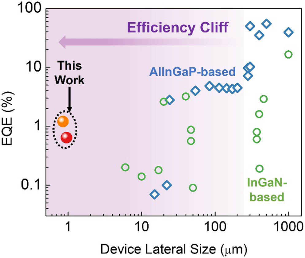
    Fig. 1. Variations of peak external quantum efficiency (EQE) of some previously reported red-emitting LEDs (defined as having emission peak >620  nm), showing the presence of the efficiency cliff, i.e., significantly reduced efficiency with decreasing device size. Blue squares: AlInGaP-based red LEDs. Green circles: InGaN-based red LEDs. The results from this work are indicated by the orange and red spheres.
    (a) Schematic illustration of N-polar InGaN/GaN nanowire LED heterostructures grown on N-polar GaN template on sapphire substrate. (b), (c) SEM images of an N-polar InGaN/GaN nanowire array, showing site-controlled epitaxy and high uniformity.
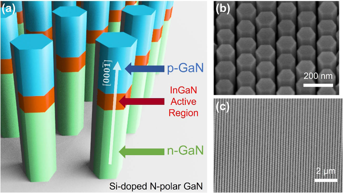
    Fig. 2. (a) Schematic illustration of N-polar InGaN/GaN nanowire LED heterostructures grown on N-polar GaN template on sapphire substrate. (b), (c) SEM images of an N-polar InGaN/GaN nanowire array, showing site-controlled epitaxy and high uniformity.
    Photoluminescence spectra of InGaN/GaN nanowire heterostructures measured at room temperature for samples with (red) and without (blue) in situ annealing. The intensity of the non-annealed sample has been enhanced by a factor of five.
    Fig. 3. Photoluminescence spectra of InGaN/GaN nanowire heterostructures measured at room temperature for samples with (red) and without (blue) in situ annealing. The intensity of the non-annealed sample has been enhanced by a factor of five.
    (a) Cross-sectional STEM-HAADF image of nanowires. (b) Magnified STEM-HAADF image of the InGaN active region in the nanowire shown in the middle of (a). (c) Atomic-scale HAADF image of the InGaN active region. (d) Color mixed element map collected from a part of the nanowire with the InGaN active region included by STEM-SI using X-ray signals showing the distributions of Ga (red) and In (green). (e) Ga and In elemental profiles along the dotted band outlined in (d), with the different sections of the nanowire shown as shaded regions.
    Fig. 4. (a) Cross-sectional STEM-HAADF image of nanowires. (b) Magnified STEM-HAADF image of the InGaN active region in the nanowire shown in the middle of (a). (c) Atomic-scale HAADF image of the InGaN active region. (d) Color mixed element map collected from a part of the nanowire with the InGaN active region included by STEM-SI using X-ray signals showing the distributions of Ga (red) and In (green). (e) Ga and In elemental profiles along the dotted band outlined in (d), with the different sections of the nanowire shown as shaded regions.
    (a) Schematic of the InGaN/GaN micro-LED device, showing current injection window before depositing p-metal contact. (b) SEM image of the submicrometer-scale device via, with the injection window indicated by the yellow dashed curve. (c) EL spectra measured for different devices, showing the tunability of the emission wavelength across the yellow-red wavelength range of the visible spectrum. For the devices shown, the sample names and the designed nanowire diameters are specified, while the nanowire pitch is kept fixed at 280 nm. (d) J-V characteristics for devices A and B, shown as orange and red curves, respectively.
    Fig. 5. (a) Schematic of the InGaN/GaN micro-LED device, showing current injection window before depositing p-metal contact. (b) SEM image of the submicrometer-scale device via, with the injection window indicated by the yellow dashed curve. (c) EL spectra measured for different devices, showing the tunability of the emission wavelength across the yellow-red wavelength range of the visible spectrum. For the devices shown, the sample names and the designed nanowire diameters are specified, while the nanowire pitch is kept fixed at 280 nm. (d) J-V characteristics for devices A and B, shown as orange and red curves, respectively.
    (a) EL spectra measured for device A from an injection current of 0.5–6 A/cm2. (b) EL spectra measured for device B from an injection current of 1–10 A/cm2. Variation of the (c) FWHM and (d) peak position, measured from the EL spectra for devices at different injection currents.
    Fig. 6. (a) EL spectra measured for device A from an injection current of 0.56  A/cm2. (b) EL spectra measured for device B from an injection current of 110  A/cm2. Variation of the (c) FWHM and (d) peak position, measured from the EL spectra for devices at different injection currents.
    Variation of EQE with current density for device A. Due to the very low power under low injection conditions, the error bar is estimated to be 15% for the derived EQE in the low current density regime.
    Fig. 7. Variation of EQE with current density for device A. Due to the very low power under low injection conditions, the error bar is estimated to be 15% for the derived EQE in the low current density regime.
    A. Pandey, Y. Malhotra, P. Wang, K. Sun, X. Liu, Z. Mi. N-polar InGaN/GaN nanowires: overcoming the efficiency cliff of red-emitting micro-LEDs[J]. Photonics Research, 2022, 10(4): 1107
    Download Citation