
A. Pandey, Y. Malhotra, P. Wang, K. Sun, X. Liu, Z. Mi, "N-polar InGaN/GaN nanowires: overcoming the efficiency cliff of red-emitting micro-LEDs," Photonics Res. 10, 1107 (2022)
- Photonics Research
- Vol. 10, Issue 4, 1107 (2022)
Abstract
1. INTRODUCTION
Sub-micrometer and nanoscale optoelectronic devices, including light emitting diodes (LEDs) and laser diodes, have drawn considerable attention, as they are essential for future large scale, or ultra-large scale integration of electronic and optoelectronic devices on a single chip. To date, however, it has remained extremely challenging to achieve high efficiency micro or nanoscale optoelectronic devices. One noticeable example is the efficiency cliff related to micro-LEDs, i.e., a drastic reduction in device efficiency with reducing dimensions. Micro-LEDs have been considered as the essential building block for emerging virtual/augmented reality devices and systems, due to their ultrahigh brightness, low power consumption, ultrahigh integration density, superior stability, and long lifetime. Shown in Fig. 1, external quantum efficiency (EQE) in the range of 50%–70% has been commonly measured for AlGaInP-based large area LEDs (lateral dimensions
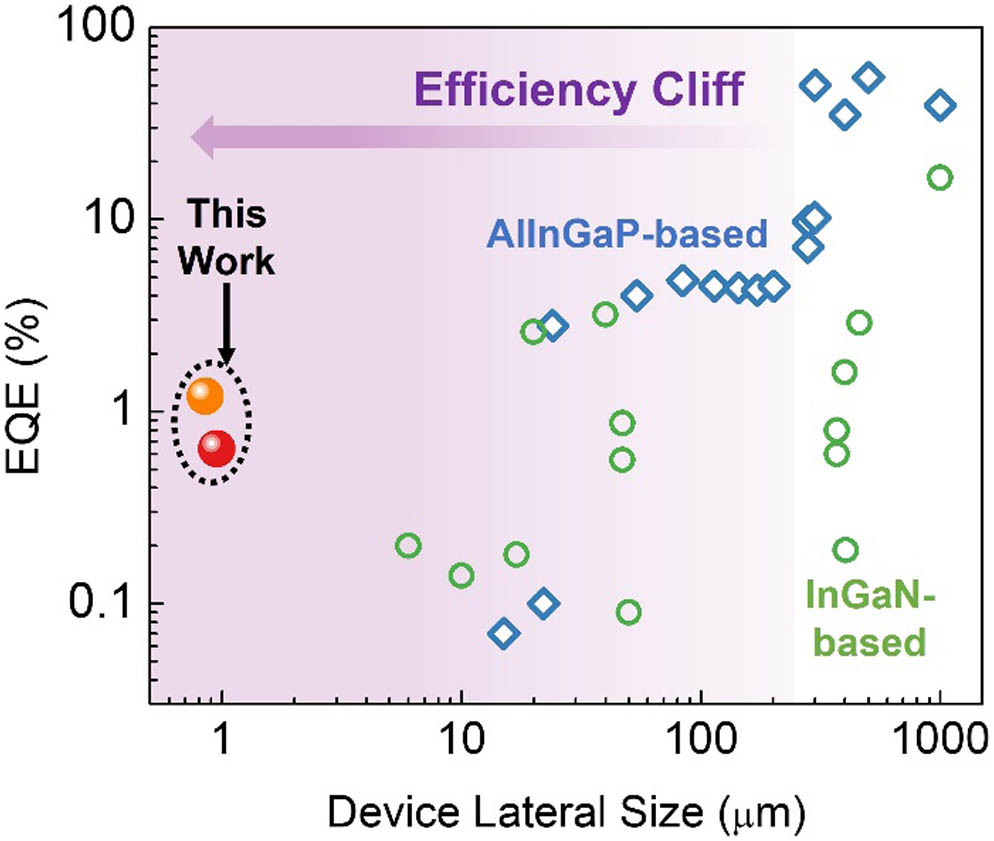
Figure 1.Variations of peak external quantum efficiency (EQE) of some previously reported red-emitting LEDs (defined as having emission peak
It is known that AlGaInP-based materials have poor charge carrier confinement, relatively long carrier diffusion length, and large surface recombination [1,2]. In this regard, Ga(In)N-based heterostructures offer stronger carrier confinement, smaller carrier diffusion lengths, as well as a lower level of surface recombination velocity [3]. However, the large lattice mismatch between InN and GaN (
In this context, bottom-up InGaN-based nanostructures, e.g., nanowires and nanorods, offer an alternative approach to overcome the efficiency cliff of micro- or nano-LEDs in the deep visible. The bottom-up approach has a major advantage over a top-down etching approach due to the reduced density of surface defects at the edge of the device mesa, commonly associated with plasma-based etching of nitrides [34–36]. (In)GaN nanostructures have been extensively studied previously, showing defect-free structures and enhanced indium incorporation because of their efficient strain relaxation [37–40]. Such InGaN-based nanostructures have shown bright luminescence over a wide spectral range due to their high internal quantum efficiency and light extraction efficiency [41–43]. Further, selective area epitaxy using a patterned mask has also been demonstrated, enabling precise control of the dimensions of nanostructures [44–46]. It has also been shown that through varying the size and spacing of nanostructures, the incorporation of In can be tuned in a single growth step, potentially enabling the monolithic growth of multi-color devices [47–50]. Previous studies on nanostructure LEDs, however, have been largely focused on InGaN-based nanowire devices with mixed or Ga polarity [51–59]. The device performance suffers severely from charge carrier (electron) overflow/leakage and nonradiative parasitic recombination outside of the device active region, leading to very low efficiency [52,60]. Moreover, the pyramid-like morphology associated with Ga-polar nanowires makes it difficult for the fabrication of high efficiency LEDs. These critical issues can be potentially addressed by N-polar InGaN-based nanowires, which are characterized by uniformly flat surfaces that are compatible with standard planar fabrication processes [61–63]. Due to the reversed polarization field in N-polar structures, electron leakage/overflow can be greatly suppressed in N-polar InGaN quantum wells/dots, compared to their Ga-polar counterparts [61]. Recent studies further suggested that the lateral surfaces of N-polar GaN nanowires can form a stable oxynitride layer, which can significantly reduce nonradiative surface recombination [64]. N-polar InGaN also exhibits a higher decomposition temperature than its metal-polar counterpart, thereby allowing for the epitaxy of InGaN at higher temperatures to reduce point defect formation and/or undesired impurity incorporation [65,66]. Despite these promises, there have been few studies of N-polar InGaN-based nanowire micro-LEDs.
Sign up for Photonics Research TOC. Get the latest issue of Photonics Research delivered right to you!Sign up now
Herein, we report, for the first time, the design, epitaxy, and performance characteristics of N-polar InGaN/GaN nanowire-based sub-micrometer scale LEDs operating in the deep visible. We have developed a unique strategy to effectively tune the emission wavelengths of N-polar InGaN/GaN nanowires. It is observed that the emission wavelengths can be shifted from yellow to orange and red by varying the material fluxes and growth temperature. It is further observed that the luminescence efficiency can be enhanced by more than one order of magnitude through an
2. SELECTIVE AREA GROWTH AND CHARACTERIZATION OF N-POLAR NANOWIRES
Schematically shown in Fig. 2(a) is the N-polar GaN/InGaN nanowire micro-LED heterostructure, which consists of Si-doped GaN, InGaN active region, and Mg-doped GaN contact layer. Prior to the epitaxy of the N-polar nanowires, Si-doped N-polar GaN templates, with thicknesses
![]()
Figure 2.(a) Schematic illustration of N-polar InGaN/GaN nanowire LED heterostructures grown on N-polar GaN template on sapphire substrate. (b), (c) SEM images of an N-polar InGaN/GaN nanowire array, showing site-controlled epitaxy and high uniformity.
Attaining efficient long wavelength emission, e.g., orange and red, for InGaN-based LEDs is extremely difficult due to the large lattice mismatch (up to 11%) between InN and GaN, indium phase separation, and quantum-confined Stark effect [68–75]. In this study, to achieve red emission, we performed a detailed investigation of the role of the In/Ga flux ratio, growth temperature for the active region, and the
The use of a relatively low growth temperature and high nitrogen flow rate in enhancing indium incorporation and achieving red emission also promotes the formation of point defects, e.g., Ga/In vacancies and N-interstitials, which may severely limit the radiative efficiency [42,77,78]. In this regard, to further improve the luminescence efficiency, we developed an
![]()
Figure 3.Photoluminescence spectra of InGaN/GaN nanowire heterostructures measured at room temperature for samples with (red) and without (blue)
A cross-sectional specimen for scanning transmission electron microscopy (STEM) study was made from a nanowire LED sample using an
Figure 4(a) is a low magnification STEM-HAADF image showing the cross section of a few nanowires. No extended crystal defects could be observed in the images of the nanowires [81]. The InGaN active region (shown as the region with a lighter contrast in the middle of the nanowire) grows axially along the c-plane of the nanowire, which contrasts with the growth along the semi-polar planes observed in Ga-polar nanowires [82–84]. While little lateral growth is observed in the nanowires until the start of the active region, following it, there is a noticeable change in nanowire diameter, which is related to the strain relaxation and relatively low growth temperature for this section [39]. The images of the nanowire arrays also show the presence of voids formed in between the nanowires, which are a result of the deposition of insulating layers to electrically isolate the nanowires. A magnified STEM-HAADF image of the InGaN active region within the nanowire in the center of Fig. 4(a) is shown in Fig. 4(b) and its atom-resolved HAADF image in Fig. 4(c). A relatively inhomogeneous InGaN segment is observed, which could be a direct consequence of the composition-pulling effect previously observed in high In composition InGaN layers [40,85,86]. In addition, the
![]()
Figure 4.(a) Cross-sectional STEM-HAADF image of nanowires. (b) Magnified STEM-HAADF image of the InGaN active region in the nanowire shown in the middle of (a). (c) Atomic-scale HAADF image of the InGaN active region. (d) Color mixed element map collected from a part of the nanowire with the InGaN active region included by STEM-SI using X-ray signals showing the distributions of Ga (red) and In (green). (e) Ga and In elemental profiles along the dotted band outlined in (d), with the different sections of the nanowire shown as shaded regions.
3. FABRICATION OF MICRO-LEDS AND DEVICE MEASUREMENTS
N-polar InGaN/GaN nanowire micro-LEDs were then fabricated. First the nanowire arrays were passivated with an insulating
![]()
Figure 5.(a) Schematic of the InGaN/GaN micro-LED device, showing current injection window before depositing p-metal contact. (b) SEM image of the submicrometer-scale device via, with the injection window indicated by the yellow dashed curve. (c) EL spectra measured for different devices, showing the tunability of the emission wavelength across the yellow-red wavelength range of the visible spectrum. For the devices shown, the sample names and the designed nanowire diameters are specified, while the nanowire pitch is kept fixed at 280 nm. (d)
Shown in Fig. 5(c), depending on the growth conditions and nanowire sizes, electroluminescence (EL) emission in the wavelength range of
EL spectra of the devices were thereafter measured at room temperature. Figure 6(a) shows the EL spectra for device A at injection currents from 0.5 to
![]()
Figure 6.(a) EL spectra measured for device A from an injection current of
For measuring the output power from the fabricated devices, we used a Keithley 2400 SMU to bias the device in continuous-wave (CW) mode, while measuring the device output power on-wafer, using a calibrated Newport 818-ST2-UV/DB detector, through the backside of the sapphire substrate. The measured EQE at different injection currents is plotted for device A, shown in Fig. 7. The EQE shows a peak at relatively low current densities of
![]()
Figure 7.Variation of EQE with current density for device A. Due to the very low power under low injection conditions, the error bar is estimated to be 15% for the derived EQE in the low current density regime.
4. SUMMARY
In summary, we have developed red-emitting N-polar InGaN/GaN nanowire heterostructures and have further demonstrated the smallest size red-emitting LEDs ever reported, to the best of our knowledge. The device surface area is nearly three orders of magnitude smaller than some of the previously reported InGaN quantum well red micro-LEDs. An EQE
Acknowledgment
Acknowledgment. Part of the TEM studies in this work were technically supported by the Michigan Center for Materials Characterization.
References
[1] J.-I. Shim, D.-P. Han, H. Kim, D.-S. Shin, G.-B. Lin, D. S. Meyaard, Q. Shan, J. Cho, E. Fred Schubert, H. Shim. Efficiency droop in AlGaInP and GaInN light-emitting diodes. Appl. Phys. Lett., 100, 111106(2012).
[2] M. S. Wong, J. A. Kearns, C. Lee, J. M. Smith, C. Lynsky, G. Lheureux, H. Choi, J. Kim, C. Kim, S. Nakamura. Improved performance of AlGaInP red micro-light-emitting diodes with sidewall treatments. Opt. Express, 28, 5787-5793(2020).
[3] M. Boroditsky, I. Gontijo, M. Jackson, R. Vrijen, E. Yablonovitch, T. Krauss, C.-C. Cheng, A. Scherer, R. Bhat, M. Krames. Surface recombination measurements on III-V candidate materials for nanostructure light-emitting diodes. J. Appl. Phys., 87, 3497-3504(2000).
[4] F. Olivier, S. Tirano, L. Dupré, B. Aventurier, C. Largeron, F. Templier. Influence of size-reduction on the performances of GaN-based micro-LEDs for display application. J. Lumin., 191, 112-116(2017).
[5] M. S. Wong, D. Hwang, A. I. Alhassan, C. Lee, R. Ley, S. Nakamura, S. P. DenBaars. High efficiency of III-nitride micro-light-emitting diodes by sidewall passivation using atomic layer deposition. Opt. Express, 26, 21324-21331(2018).
[6] D. Hwang, A. Mughal, C. D. Pynn, S. Nakamura, S. P. DenBaars. Sustained high external quantum efficiency in ultrasmall blue III–nitride micro-LEDs. Appl. Phys. Express, 10, 032101(2017).
[7] F. Olivier, A. Daami, C. Licitra, F. Templier. Shockley-Read-Hall and Auger non-radiative recombination in GaN based LEDs: a size effect study. Appl. Phys. Lett., 111, 022104(2017).
[8] K. A. Bulashevich, S. Y. Karpov. Impact of surface recombination on efficiency of III-nitride light-emitting diodes. Phys. Status Solidi RRL, 10, 480-484(2016).
[9] E. F. Schubert. Light-Emitting Diodes(2006).
[10] S. Zhang, J. Zhang, J. Gao, X. Wang, C. Zheng, M. Zhang, X. Wu, L. Xu, J. Ding, Z. Quan. Efficient emission of InGaN-based light-emitting diodes: toward orange and red. Photon. Res., 8, 1671-1675(2020).
[11] J.-I. Hwang, R. Hashimoto, S. Saito, S. Nunoue. Development of InGaN-based red LED grown on (0001) polar surface. Appl. Phys. Express, 7, 071003(2014).
[12] D. Iida, K. Niwa, S. Kamiyama, K. Ohkawa. Demonstration of InGaN-based orange LEDs with hybrid multiple-quantum-wells structure. Appl. Phys. Express, 9, 111003(2016).
[13] D. Iida, Z. Zhuang, P. Kirilenko, M. Velazquez-Rizo, M. A. Najmi, K. Ohkawa. 633-nm InGaN-based red LEDs grown on thick underlying GaN layers with reduced in-plane residual stress. Appl. Phys. Lett., 116, 162101(2020).
[14] D. Iida, Z. Zhuang, P. Kirilenko, M. Velazquez-Rizo, K. Ohkawa. Demonstration of low forward voltage InGaN-based red LEDs. Appl. Phys. Express, 13, 031001(2020).
[15] S. S. Pasayat, C. Gupta, M. S. Wong, R. Ley, M. J. Gordon, S. P. DenBaars, S. Nakamura, S. Keller, U. K. Mishra. Demonstration of ultra-small (<10 μm) 632 nm red InGaN micro-LEDs with useful on-wafer external quantum efficiency (>0.2%) for mini-displays. Appl. Phys. Express, 14, 011004(2021).
[16] A. Dussaigne, P. L. Maitre, H. Haas, J.-C. Pillet, F. Barbier, A. Grenier, N. Michit, A. Jannaud, R. Templier, D. Vaufrey, F. Rol, O. Ledoux, D. Sotta. Full InGaN red (625 nm) micro-LED (10 μm) demonstration on a relaxed pseudo-substrate. Appl. Phys. Express, 14, 092011(2021).
[17] D. Iida, S. Lu, S. Hirahara, K. Niwa, S. Kamiyama, K. Ohkawa. Enhanced light output power of InGaN-based amber LEDs by strain-compensating AlN/AlGaN barriers. J. Cryst. Growth, 448, 105-108(2016).
[18] A. Dussaigne, F. Barbier, B. Damilano, S. Chenot, A. Grenier, A. Papon, B. Samuel, B. Ben Bakir, D. Vaufrey, J. Pillet, A. Gasse, O. Ledoux, M. Rozhavskaya, D. Sotta. Full InGaN red light emitting diodes. J. Appl. Phys., 128, 135704(2020).
[19] Z. Zhuang, D. Iida, K. Ohkawa. Investigation of InGaN-based red/green micro-light-emitting diodes. Opt. Lett., 46, 1912-1915(2021).
[20] P. Li, A. David, H. Li, H. Zhang, C. Lynsky, Y. Yang, M. Iza, J. S. Speck, S. Nakamura, S. P. DenBaars. High-temperature electroluminescence properties of InGaN red 40 × 40 μm2 micro-light-emitting diodes with a peak external quantum efficiency of 3.2%. Appl. Phys. Lett., 119, 231101(2021).
[21] Z. Zhuang, D. Iida, M. Velazquez-Rizo, K. Ohkawa. 630-nm red InGaN micro-light-emitting diodes (<20 μm × 20 μm) exceeding 1 mW/mm2 for full-color micro-displays. Photon. Res., 9, 1796-1802(2021).
[22] P. Li, H. Li, H. Zhang, C. Lynsky, M. Iza, J. S. Speck, S. Nakamura, S. P. DenBaars. Size-independent peak external quantum efficiency (>2%) of InGaN red micro-light-emitting diodes with an emission wavelength over 600 nm. Appl. Phys. Lett., 119, 081102(2021).
[23] Z. Zhuang, D. Iida, P. Kirilenko, K. Ohkawa. Improved performance of InGaN-based red light-emitting diodes by micro-hole arrays. Opt. Express, 29, 29780-29788(2021).
[24] K. Streubel, U. Helin, V. Oskarsson, E. Bäcklin, Å. Johansson. High brightness visible (660 nm) resonant-cavity light-emitting diode. IEEE Photon. Technol. Lett., 10, 1685-1687(1998).
[25] C. Y. Lee, J. Y. Su, C. M. Kuo. 630-nm n-type modulation-doped AlGaInP-AlInP multiquantum-well light-emitting diode. IEEE Photon. Technol. Lett., 18, 25-27(2006).
[26] R. Windisch, R. Butendeich, S. Illek, S. Kugler, R. Wirth, H. Zull, K. Streubel. 100-lm/W InGaAlP thin-film light-emitting diodes with buried microreflectors. IEEE Photon. Technol. Lett., 19, 774-776(2007).
[27] C. Rooman, S. D. Jonge, C. Karnutsch, K. Streubel, M. Kuijk, B. Dutta, G. Borghs, P. L. Heremans. Wafer-bonded thin-film surface-roughened light-emitting diodes. Proc. SPIE, 4996, 40-45(2003).
[28] M. R. Krames, M. Ochiai-Holcomb, G. Höfler, C. Carter-Coman, E. Chen, I.-H. Tan, P. Grillot, N. Gardner, H. Chui, J.-W. Huang. High-power truncated-inverted-pyramid (Al
[29] X.-L. Wang, N. Kumagai, G.-D. Hao. High-efficiency, high-power AlGaInP thin-film LEDs with micron-sized truncated cones as light-extraction structures. Phys. Status Solidi A, 215, 1700562(2018).
[30] J.-T. Oh, S.-Y. Lee, Y.-T. Moon, J. H. Moon, S. Park, K. Y. Hong, K. Y. Song, C. Oh, J.-I. Shim, H.-H. Jeong. Light output performance of red AlGaInP-based light emitting diodes with different chip geometries and structures. Opt. Express, 26, 11194-11200(2018).
[31] C. H. Yen, Y. J. Liu, K. H. Yu, P. L. Lin, T. P. Chen, L. Y. Chen, T. H. Tsai, N. Y. Huang, C. Y. Lee, W. C. Liu. On an AlGaInP-based light-emitting diode with an ITO direct ohmic contact structure. IEEE Electron Device Lett., 30, 359-361(2009).
[32] R. Wirth, C. Karnutsch, S. Kugler, K. Streubel. High-efficiency resonant-cavity LEDs emitting at 650 nm. IEEE Photon. Technol. Lett., 13, 421-423(2001).
[33] D. Malacara. Color Vision and Colorimetry: Theory and Applications(2011).
[34] R. Qiu, H. Lu, D. Chen, R. Zhang, Y. Zheng. Optimization of inductively coupled plasma deep etching of GaN and etching damage analysis. Appl. Surf. Sci., 257, 2700-2706(2011).
[35] J. Ladroue, A. Meritan, M. Boufnichel, P. Lefaucheux, P. Ranson, R. Dussart. Deep GaN etching by inductively coupled plasma and induced surface defects. J. Vac. Sci. Technol. A, 28, 1226-1233(2010).
[36] M. Hartensveld, G. Ouin, C. Liu, J. Zhang. Effect of KOH passivation for top-down fabricated InGaN nanowire light emitting diodes. J. Appl. Phys., 126, 183102(2019).
[37] E. Ertekin, P. A. Greaney, D. Chrzan, T. D. Sands. Equilibrium limits of coherency in strained nanowire heterostructures. J. Appl. Phys., 97, 114325(2005).
[38] F. Glas. Critical dimensions for the plastic relaxation of strained axial heterostructures in free-standing nanowires. Phys. Rev. B, 74, 121302(2006).
[39] G. Tourbot, C. Bougerol, F. Glas, L. F. Zagonel, Z. Mahfoud, S. Meuret, P. Gilet, M. Kociak, B. Gayral, B. Daudin. Growth mechanism and properties of InGaN insertions in GaN nanowires. Nanotechnology, 23, 135703(2012).
[40] G. Tourbot, C. Bougerol, A. Grenier, M. Den Hertog, D. Sam-Giao, D. Cooper, P. Gilet, B. Gayral, B. Daudin. Structural and optical properties of InGaN/GaN nanowire heterostructures grown by PA-MBE. Nanotechnology, 22, 075601(2011).
[41] K. Kishino, A. Kikuchi, H. Sekiguchi, S. Ishizawa. InGaN/GaN nanocolumn LEDs emitting from blue to red. Proc. SPIE, 6473, 64730T(2007).
[42] X. Zhang, H. Lourenço-Martins, S. Meuret, M. Kociak, B. Haas, J.-L. Rouvière, P.-H. Jouneau, C. Bougerol, T. Auzelle, D. Jalabert. InGaN nanowires with high InN molar fraction: growth, structural and optical properties. Nanotechnology, 27, 195704(2016).
[43] S. Deshpande, T. Frost, L. Yan, S. Jahangir, A. Hazari, X. Liu, J. Mirecki-Millunchick, Z. Mi, P. Bhattacharya. Formation and nature of InGaN quantum dots in GaN nanowires. Nano Lett., 15, 1647-1653(2015).
[44] H. Sekiguchi, K. Kishino, A. Kikuchi. Ti-mask selective-area growth of GaN by RF-plasma-assisted molecular-beam epitaxy for fabricating regularly arranged InGaN/GaN nanocolumns. Appl. Phys. Express, 1, 124002(2008).
[45] K. Kishino, T. Hoshino, S. Ishizawa, A. Kikuchi. Selective-area growth of GaN nanocolumns on titanium-mask-patterned silicon (111) substrates by RF-plasma-assisted molecular-beam epitaxy. Electron. Lett., 44, 819-821(2008).
[46] S. D. Hersee, X. Sun, X. Wang. The controlled growth of GaN nanowires. Nano Lett., 6, 1808-1811(2006).
[47] H. Sekiguchi, K. Kishino, A. Kikuchi. Emission color control from blue to red with nanocolumn diameter of InGaN/GaN nanocolumn arrays grown on same substrate. Appl. Phys. Lett., 96, 231104(2010).
[48] K. Kishino, A. Yanagihara, K. Ikeda, K. Yamano. Monolithic integration of four-colour InGaN-based nanocolumn LEDs. Electron. Lett., 51, 852-854(2015).
[49] K. Kishino, K. Nagashima, K. Yamano. Monolithic integration of InGaN-based nanocolumn light-emitting diodes with different emission colors. Appl. Phys. Express, 6, 012101(2012).
[50] Y.-H. Ra, R. Wang, S. Y. Woo, M. Djavid, S. M. Sadaf, J. Lee, G. A. Botton, Z. Mi. Full-color single nanowire pixels for projection displays. Nano Lett., 16, 4608-4615(2016).
[51] H. P. T. Nguyen, K. Cui, S. Zhang, S. Fathololoumi, Z. Mi. Full-color InGaN/GaN dot-in-a-wire light emitting diodes on silicon. Nanotechnology, 22, 445202(2011).
[52] H. P. T. Nguyen, M. Djavid, S. Y. Woo, X. Liu, A. T. Connie, S. Sadaf, Q. Wang, G. A. Botton, I. Shih, Z. Mi. Engineering the carrier dynamics of InGaN nanowire white light-emitting diodes by distributed p-AlGaN electron blocking layers. Sci. Rep., 5, 7744(2015).
[53] C. Zhao, N. Alfaraj, R. C. Subedi, J. W. Liang, A. A. Alatawi, A. A. Alhamoud, M. Ebaid, M. S. Alias, T. K. Ng, B. S. Ooi. III-nitride nanowires on unconventional substrates: From materials to optoelectronic device applications. Prog. Quantum Electron., 61, 1-31(2018).
[54] M. Asad, R. Wang, Y.-H. Ra, P. Gavirneni, Z. Mi, W. S. Wong. Optically invariant InGaN nanowire light-emitting diodes on flexible substrates under mechanical manipulation. npj Flexible Electron., 3, 16(2019).
[55] R. Wang, X. Liu, I. Shih, Z. Mi. High efficiency, full-color AlInGaN quaternary nanowire light emitting diodes with spontaneous core-shell structures on Si. Appl. Phys. Lett., 106, 261104(2015).
[56] H. P. T. Nguyen, S. Zhang, A. T. Connie, M. G. Kibria, Q. Wang, I. Shih, Z. Mi. Breaking the carrier injection bottleneck of phosphor-free nanowire white light-emitting diodes. Nano Lett., 13, 5437-5442(2013).
[57] M. Nami, A. Rashidi, M. Monavarian, S. Mishkat-Ul-Masabih, A. K. Rishinaramangalam, S. R. Brueck, D. Feezell. Electrically injected GHz-class GaN/InGaN core–shell nanowire-based μLEDs: carrier dynamics and nanoscale homogeneity. ACS Photon., 6, 1618-1625(2019).
[58] M. Philip, D. Choudhary, M. Djavid, K. Le, J. Piao, H. Nguyen. High efficiency green/yellow and red InGaN/AlGaN nanowire light-emitting diodes grown by molecular beam epitaxy. J. Sci.: Adv. Mater. Devices, 2, 150-155(2017).
[59] G. Zhang, Z. Li, X. Yuan, F. Wang, L. Fu, Z. Zhuang, F.-F. Ren, B. Liu, R. Zhang, H. H. Tan. Single nanowire green InGaN/GaN light emitting diodes. Nanotechnology, 27, 435205(2016).
[60] H. P. T. Nguyen, K. Cui, S. Zhang, M. Djavid, A. Korinek, G. A. Botton, Z. Mi. Controlling electron overflow in phosphor-free InGaN/GaN nanowire white light-emitting diodes. Nano Lett., 12, 1317-1323(2012).
[61] F. Akyol, D. Nath, S. Krishnamoorthy, P. Park, S. Rajan. Suppression of electron overflow and efficiency droop in N-polar GaN green light emitting diodes. Appl. Phys. Lett., 100, 111118(2012).
[62] Y.-K. Kuo, S.-H. Horng, S.-H. Yen, M.-C. Tsai, M.-F. Huang. Effect of polarization state on optical properties of blue-violet InGaN light-emitting diodes. Appl. Phys. A, 98, 509-515(2010).
[63] S.-H. Yen, Y.-K. Kuo. Polarization-dependent optical characteristics of violet InGaN laser diodes. J. Appl. Phys., 103, 103115(2008).
[64] G. Zeng, T. A. Pham, S. Vanka, G. Liu, C. Song, J. K. Cooper, Z. Mi, T. Ogitsu, F. M. Toma. Development of a photoelectrochemically self-improving Si/GaN photocathode for efficient and durable H 2 production. Nat. Mater., 20, 1130-1135(2021).
[65] S. Keller, N. Fichtenbaum, M. Furukawa, J. Speck, S. DenBaars, U. Mishra. Growth and characterization of N-polar InGaN/GaN multiquantum wells. Appl. Phys. Lett., 90, 191908(2007).
[66] D. N. Nath, E. Gür, S. A. Ringel, S. Rajan. Molecular beam epitaxy of N-polar InGaN. Appl. Phys. Lett., 97, 071903(2010).
[67] P. Wang, D. Wang, B. Wang, S. Mohanty, S. Diez, Y. Wu, Y. Sun, E. Ahmadi, Z. Mi. N-polar ScAlN and HEMTs grown by molecular beam epitaxy. Appl. Phys. Lett., 119, 082101(2021).
[68] M. H. Crawford. LEDs for solid-state lighting: performance challenges and recent advances. IEEE J. Sel. Top. Quantum Electron., 15, 1028-1040(2009).
[69] T. Mukai, M. Yamada, S. Nakamura. Characteristics of InGaN-based UV/blue/green/amber/red light-emitting diodes. Jpn. J. Appl. Phys., 38, 3976(1999).
[70] T. Langer, A. Kruse, F. A. Ketzer, A. Schwiegel, L. Hoffmann, H. Jönen, H. Bremers, U. Rossow, A. Hangleiter. Origin of the “green gap”: Increasing nonradiative recombination in indium-rich GaInN/GaN quantum well structures. Phys. Status Solidi C, 8, 2170-2172(2011).
[71] M. Rao, D. Kim, S. Mahajan. Compositional dependence of phase separation in InGaN layers. Appl. Phys. Lett., 85, 1961-1963(2004).
[72] B. Pantha, J. Li, J. Lin, H. Jiang. Evolution of phase separation in In-rich InGaN alloys. Appl. Phys. Lett., 96, 232105(2010).
[73] I. H. Ho, G. Stringfellow. Solid phase immiscibility in GaInN. Appl. Phys. Lett., 69, 2701-2703(1996).
[74] T. Takeuchi, S. Sota, M. Katsuragawa, M. Komori, H. Takeuchi, H. Amano, I. Akasaki. Quantum-confined Stark effect due to piezoelectric fields in GaInN strained quantum wells. Jpn. J. Appl. Phys., 36, L382(1997).
[75] J. Wu. When group-III nitrides go infrared: new properties and perspectives. J. Appl. Phys., 106, 011101(2009).
[76] A. Trampert, O. Brandt, K. Ploog. Crystal structure of group III nitrides. Semiconductors and Semimetals, 50, 167-192(1997).
[77] D. A. Browne, E. C. Young, J. R. Lang, C. A. Hurni, J. S. Speck. Indium and impurity incorporation in InGaN films on polar, nonpolar, and semipolar GaN orientations grown by ammonia molecular beam epitaxy. J. Vac. Sci. Technol. A, 30, 041513(2012).
[78] H. Komaki, T. Nakamura, R. Katayama, K. Onabe, M. Ozeki, T. Ikari. Growth of In-rich InGaN films on sapphire via GaN layer by RF-MBE. J. Cryst. Growth, 301, 473-477(2007).
[79] N. A. Kaufmann, A. Dussaigne, D. Martin, P. Valvin, T. Guillet, B. Gil, F. Ivaldi, S. Kret, N. Grandjean. Thermal annealing of molecular beam epitaxy-grown InGaN/GaN single quantum well. Semicond. Sci. Technol., 27, 105023(2012).
[80] C.-C. Chuo, C.-M. Lee, T.-E. Nee, J.-I. Chyi. Effects of thermal annealing on the luminescence and structural properties of high indium-content InGaN/GaN quantum wells. Appl. Phys. Lett., 76, 3902-3904(2000).
[81] S. Y. Woo, M. Bugnet, H. P. Nguyen, Z. Mi, G. A. Botton. Atomic ordering in InGaN alloys within nanowire heterostructures. Nano Lett., 15, 6413-6418(2015).
[82] Y.-H. Ra, R. T. Rashid, X. Liu, S. M. Sadaf, K. Mashooq, Z. Mi. An electrically pumped surface-emitting semiconductor green laser. Sci. Adv., 6, eaav7523(2020).
[83] L. Nicolai, Ž. Gačević, E. Calleja, A. Trampert. Electron tomography of pencil-shaped GaN/(In,Ga)N core-shell nanowires. Nano. Res. Lett., 14, 232(2019).
[84] Z. A. Gačević, M. Holmes, E. Chernysheva, M. Müller, A. Torres-Pardo, P. Veit, F. Bertram, J. R. Christen, J. M. A. González Calbet, Y. Arakawa. Emission of linearly polarized single photons from quantum dots contained in nonpolar, semipolar, and polar sections of pencil-like InGaN/GaN nanowires. ACS Photon., 4, 657-664(2017).
[85] G. Stringfellow. The importance of lattice mismatch in the growth of Ga
[86] Y. Kawaguchi, M. Shimizu, M. Yamaguchi, K. Hiramatsu, N. Sawaki, W. Taki, H. Tsuda, N. Kuwano, K. Oki, T. Zheleva. The formation of crystalline defects and crystal growth mechanism in In
[87] D. Queren, M. Schillgalies, A. Avramescu, G. Brüderl, A. Laubsch, S. Lutgen, U. Strauß. Quality and thermal stability of thin InGaN films. J. Cryst. Growth, 311, 2933-2936(2009).
[88] C.-C. Chuo, M. N. Chang, F.-M. Pan, C.-M. Lee, J.-I. Chyi. Effect of composition inhomogeneity on the photoluminescence of InGaN/GaN multiple quantum wells upon thermal annealing. Appl. Phys. Lett., 80, 1138-1140(2002).
[89] C.-C. Chuo, C.-M. Lee, J.-I. Chyi. Interdiffusion of In and Ga in InGaN/GaN multiple quantum wells. Appl. Phys. Lett., 78, 314-316(2001).
[90] H. Wang, Z. Ji, S. Qu, G. Wang, Y. Jiang, B. Liu, X. Xu, H. Mino. Influence of excitation power and temperature on photoluminescence in InGaN/GaN multiple quantum wells. Opt. Express, 20, 3932-3940(2012).
[91] S. Marcinkevičius, K. Gelžinytė, Y. Zhao, S. Nakamura, S. DenBaars, J. Speck. Carrier redistribution between different potential sites in semipolar (
[92] S. Chichibu, T. Azuhata, T. Sota, S. Nakamura. Spontaneous emission of localized excitons in InGaN single and multiquantum well structures. Appl. Phys. Lett., 69, 4188-4190(1996).
[93] Y. Robin, M. Pristovsek, H. Amano, F. Oehler, R. Oliver, C. Humphreys. What is red? On the chromaticity of orange-red InGaN/GaN based LEDs. J. Appl. Phys., 124, 183102(2018).
[94] Y. H. Ra, R. T. Rashid, X. Liu, J. Lee, Z. Mi. Scalable nanowire photonic crystals: Molding the light emission of InGaN. Adv. Funct. Mater., 27, 1702364(2017).
[95] X. Liu, Y. Wu, Y. Malhotra, Y. Sun, Z. Mi. Micrometer scale InGaN green light emitting diodes with ultra-stable operation. Appl. Phys. Lett., 117, 011104(2020).
[96] C. Zhao, T. K. Ng, A. Prabaswara, M. Conroy, S. Jahangir, T. Frost, J. O’Connell, J. D. Holmes, P. J. Parbrook, P. Bhattacharya. An enhanced surface passivation effect in InGaN/GaN disk-in-nanowire light emitting diodes for mitigating Shockley–Read–Hall recombination. Nanoscale, 7, 16658-16665(2015).
[97] W. Liu, D. Zhao, D. Jiang, P. Chen, Z. Liu, J. Zhu, X. Li, F. Liang, J. Liu, L. Zhang. Shockley–Read–Hall recombination and efficiency droop in InGaN/GaN multiple-quantum-well green light-emitting diodes. J. Phys. D, 49, 145104(2016).
[98] X. Liu, Y. Sun, Y. Malhotra, A. Pandey, Y. Wu, K. Sun, Z. Mi. High efficiency InGaN nanowire tunnel junction green micro-LEDs. Appl. Phys. Lett., 119, 141110(2021).
[99] X. Liu, K. Mashooq, T. Szkopek, Z. Mi. Improving the efficiency of transverse magnetic polarized emission from AlGaN based LEDs by using nanowire photonic crystal. IEEE Photon. J., 10, 4501211(2018).
[100] M. G. Kibria, R. Qiao, W. Yang, I. Boukahil, X. Kong, F. A. Chowdhury, M. L. Trudeau, W. Ji, H. Guo, F. Himpsel. Atomic-scale origin of long-term stability and high performance of p-GaN nanowire arrays for photocatalytic overall pure water splitting. Adv. Mater., 28, 8388-8397(2016).
[101] A. David, M. J. Grundmann. Droop in InGaN light-emitting diodes: a differential carrier lifetime analysis. Appl. Phys. Lett., 96, 103504(2010).
[102] A. Laubsch, M. Sabathil, W. Bergbauer, M. Strassburg, H. Lugauer, M. Peter, S. Lutgen, N. Linder, K. Streubel, J. Hader. On the origin of IQE-‘droop’ in InGaN LEDs. Phys. Status Solidi C, 6, S913-S916(2009).
[103] G. Verzellesi, D. Saguatti, M. Meneghini, F. Bertazzi, M. Goano, G. Meneghesso, E. Zanoni. Efficiency droop in InGaN/GaN blue light-emitting diodes: physical mechanisms and remedies. J. Appl. Phys., 114, 071101(2013).
[104] H. Zhao, G. Liu, R. A. Arif, N. Tansu. Current injection efficiency induced efficiency-droop in InGaN quantum well light-emitting diodes. Solid-State Electron., 54, 1119-1124(2010).
[105] J. Iveland, L. Martinelli, J. Peretti, J. S. Speck, C. Weisbuch. Direct measurement of Auger electrons emitted from a semiconductor light-emitting diode under electrical injection: identification of the dominant mechanism for efficiency droop. Phys. Rev. Lett., 110, 177406(2013).
[106] X. Liu, Y. Sun, Y. Malhotra, A. Pandey, P. Wang, Y. Wu, K. Sun, Z. Mi. N-polar InGaN nanowires: breaking the efficiency bottleneck of nano and micro LEDs. Photon. Res., 10, 587-593(2021).
[107] J. Wang, E. C. Young, W. Y. Ho, B. Bonef, T. Margalith, J. S. Speck. III-nitride blue light-emitting diodes utilizing hybrid tunnel junction with low excess voltage. Semicond. Sci. Technol., 35, 125026(2020).


Set citation alerts for the article
Please enter your email address

© Copyright 2018-2021 | Chinese Laser Press. All Rights Reserved 沪ICP备15018463号-20