• Photonics Research
  • Vol. 9, Issue 4, 521 (2021)
Xue Wang1、2, Junfeng Jiang1、3、*, Shuang Wang1、4、*, Kun Liu1, and Tiegen Liu1、5、*
Author Affiliations
  • 1School of Precision Instrument and Opto-electronics Engineering, Tianjin Optical Fiber Sensing Engineering Center, Institute of Optical Fiber Sensing of Tianjin University, Key Laboratory of Opto-electronics Information Technology, Tianjin University, Tianjin 300072, China
  • 2School of Electrical and Electronic Engineering, Engineering Research Center of Optoelectronic Devices and Communication Technology, Ministry of Education, Tianjin Key Laboratory of Film Electronic and Communication Devices, Tianjin University of Technology, Tianjin 300384, China
  • 3e-mail: jiangjfjxu@tju.edu.cn
  • 4e-mail: shuangwang@tju.edu.cn
  • 5e-mail: tgliu@tju.edu.cn
  • show less
    DOI: 10.1364/PRJ.414121 Cite this Article Set citation alerts
    Xue Wang, Junfeng Jiang, Shuang Wang, Kun Liu, Tiegen Liu. All-silicon dual-cavity fiber-optic pressure sensor with ultralow pressure-temperature cross-sensitivity and wide working temperature range[J]. Photonics Research, 2021, 9(4): 521 Copy Citation Text show less
    (a) Schematic diagram of the all-silicon-based dual-cavity fiber-optic pressure sensor structure. (All the components are high-temperature resistant materials.) (b) Interference model of the dual-cavity structure with three reflective mirrors; (c) simulation of reflected spectra IR(λ). (Simulation parameters: n1=1, n2=3.47, L1=60 μm, L2=300 μm, I0 is a broadband light source with a central wavelength of 1550 nm.)
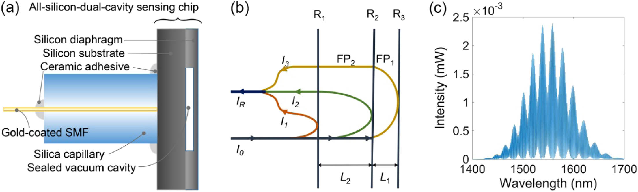
    Fig. 1. (a) Schematic diagram of the all-silicon-based dual-cavity fiber-optic pressure sensor structure. (All the components are high-temperature resistant materials.) (b) Interference model of the dual-cavity structure with three reflective mirrors; (c) simulation of reflected spectra IR(λ). (Simulation parameters: n1=1, n2=3.47, L1=60  μm, L2=300  μm, I0 is a broadband light source with a central wavelength of 1550 nm.)
    All-silicon sensing chip’s mechanical deformation when external pressure and residual pressure are applied to it. Schematic diagram of the length and thickness of each part of the sensing chip.
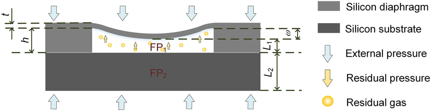
    Fig. 2. All-silicon sensing chip’s mechanical deformation when external pressure and residual pressure are applied to it. Schematic diagram of the length and thickness of each part of the sensing chip.
    Simulation results of the nonlinear response characters of the sensor model based on anodic bonding. (a) OPD response of FP1 with the variation of temperature and pressure; (b) pressure measurement errors of FP1 by using the traditional linear compensation method.
    Fig. 3. Simulation results of the nonlinear response characters of the sensor model based on anodic bonding. (a) OPD response of FP1 with the variation of temperature and pressure; (b) pressure measurement errors of FP1 by using the traditional linear compensation method.
    Fabrication processes of the proposed FPI sensing chip. (a) Spin the photoresist on the surface of the device layer of the SOI wafer; (b) photolithograph with the pre-prepared mask; (c) etch the cavity array by dry etching; (d) remove the photoresist; (e) prebond the SOI wafer with the silicon wafer; (f) anneal the prebonded wafer; (g) remove the handle layer and buried oxide layer by dry etching; (h) roughen the surface of the device layer by ultraviolet laser; (i) dice the bonded wafer into independent sensing chips; (j) assemble the sensing chip with silica capillary and gold-coated SMF.
    Fig. 4. Fabrication processes of the proposed FPI sensing chip. (a) Spin the photoresist on the surface of the device layer of the SOI wafer; (b) photolithograph with the pre-prepared mask; (c) etch the cavity array by dry etching; (d) remove the photoresist; (e) prebond the SOI wafer with the silicon wafer; (f) anneal the prebonded wafer; (g) remove the handle layer and buried oxide layer by dry etching; (h) roughen the surface of the device layer by ultraviolet laser; (i) dice the bonded wafer into independent sensing chips; (j) assemble the sensing chip with silica capillary and gold-coated SMF.
    Pictures of different parts of the fiber-optic pressure sensor structure. (a) Complete sensor after the MEMS process and package; (b) sectional view of a sensing chip and the inset is the detailed section view under a microscope; and (c) top view of the whole wafer before being roughened.
    Fig. 5. Pictures of different parts of the fiber-optic pressure sensor structure. (a) Complete sensor after the MEMS process and package; (b) sectional view of a sensing chip and the inset is the detailed section view under a microscope; and (c) top view of the whole wafer before being roughened.
    Experimental configuration for investigation of the pressure characteristic of the sensor.
    Fig. 6. Experimental configuration for investigation of the pressure characteristic of the sensor.
    Example of the demodulation process from the reflection spectra. (a) Recorded interference spectra under 20°C and 100 kPa; (b) OPD results after taking fast Fourier transform of the reflection spectra.
    Fig. 7. Example of the demodulation process from the reflection spectra. (a) Recorded interference spectra under 20°C and 100 kPa; (b) OPD results after taking fast Fourier transform of the reflection spectra.
    Demodulation results of OPDs’ response to pressure from 20 to 280 kPa at low temperatures. The demodulation results corresponding to (a) vacuum cavity FP1 and (b) silicon cavity FP2.
    Fig. 8. Demodulation results of OPDs’ response to pressure from 20 to 280 kPa at low temperatures. The demodulation results corresponding to (a) vacuum cavity FP1 and (b) silicon cavity FP2.
    Experimental configuration for the investigation of the high-temperature characters of the sensor.
    Fig. 9. Experimental configuration for the investigation of the high-temperature characters of the sensor.
    Demodulation results of OPDs’ response to high temperature from 100°C to 700°C under atmosphere environment. The demodulation results corresponding to (a) vacuum cavity FP1 and (b) silicon cavity FP2.
    Fig. 10. Demodulation results of OPDs’ response to high temperature from 100°C to 700°C under atmosphere environment. The demodulation results corresponding to (a) vacuum cavity FP1 and (b) silicon cavity FP2.
    TypeStructurePressure SensitivityTemperature Cross-SensitivityPressure-Temperature Cross-Sensitivity
    MEMSThe present work33.034 nm/kPa0.197 nm/°C5.96 Pa/°C
    Silicon-glass-silicon double-sided anodic bonding [15]12.816 nm/kPa3.365 nm/°C263 Pa/°C
    Silicon-glass anodic bonding [16]3  nm/kPa1.136  nm/°C379  Pa/°C
    Silicon-glass thermal compression bonding [14]47.26 nm/kPa3.4 nm/°C71.9 Pa/°C
    All sapphire direct bonding [13]5.122  nm/kPa2.5  nm/°C488  Pa/°C
    All-silicaSMF-MMF-silica diaphragm [25]24.8 nm/kPa1.48 nm/°C60 Pa/°C
    SMF-HC-PBF-HCF [26]1.336 nm/kPa0.1 nm/°C74 Pa/°C
    Fiber-tip air bubble FPI [27]24.44 nm/kPa2.6 nm/°C106 Pa/°C
    SMF with side-open F–P cavity [28]4.071 pm/kPa (wavelength shift)0.83 pm/°C (wavelength shift)204 Pa/°C
    SMF fabricated by femtosecond laser [29]0.56 nm/kPa8.88×103  nm/°C15.86 Pa/°C
    Table 1. Comparison of the Proposed Fiber-Optic Pressure Sensors in Terms of Structure, Pressure Sensitivity, Temperature Cross-Sensitivity, and Pressure-Temperature Cross-Sensitivity
    Xue Wang, Junfeng Jiang, Shuang Wang, Kun Liu, Tiegen Liu. All-silicon dual-cavity fiber-optic pressure sensor with ultralow pressure-temperature cross-sensitivity and wide working temperature range[J]. Photonics Research, 2021, 9(4): 521
    Download Citation