
Lijuan Wu, Shaolian Su, Xing Chen, Jinsheng Zeng, Haifeng Wu. A deep trench super-junction LDMOS with double charge compensation layer[J]. Journal of Semiconductors, 2022, 43(10): 104102
- Journal of Semiconductors
- Vol. 43, Issue 10, 104102 (2022)
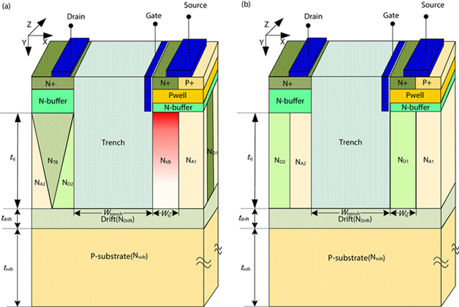
Fig. 1. (Color online) The structure of (a) DC DT SJ LDMOS and (b) Con. DT SJ LDMOS.
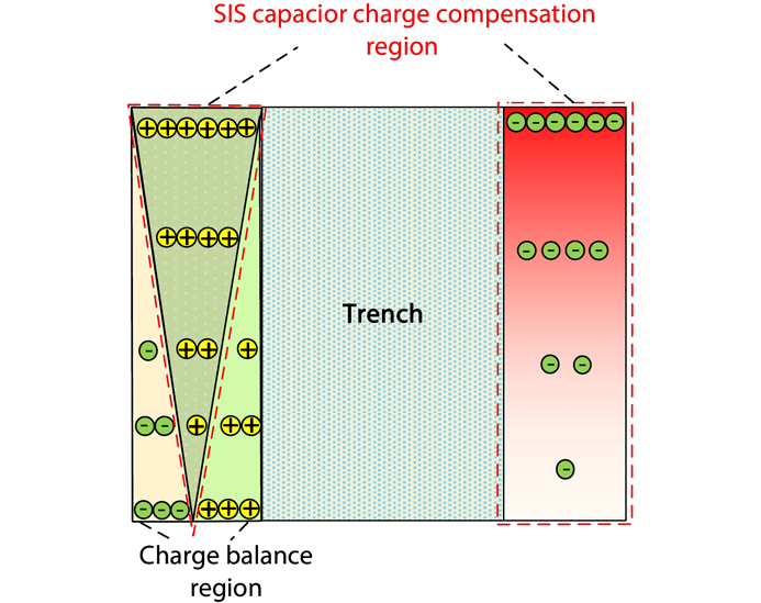
Fig. 2. (Color online) Structure and composition of the DC DT SJ LDMOS.
Fig. 3. (Color online) The influence ofNsj at source on BV of Con. DT SJ LDMOS and DC DT SJ LDMOS.
Fig. 4. (Color online) The influence ofNsj2 at the drain on BV of DC DT SJ LDMOS.
Fig. 5. (Color online) The influence ofNTB at the drain on BV of DC DT SJ LDMOS.
Fig. 6. (Color online) The influence ofNVB on BV of DC DT SJ LDMOS. (a) Influence ofNVB, max on BV of DC DT SJ LDMOS. (b) Influence ofNVB,min on BV of DC DT SJ LDMOS.
Fig. 7. (Color online) The influence ofNdrift on BV and FOM of Con. DT SJ LDMOS and DC DT SJ LDMOS.
Fig. 8. (Color online) The distribution of equipotential lines in the off state of (a) Con. DT SJ LDMOS, (b) DC DT SJ LDMOS.
Fig. 9. (Color online) The surface electric field (Y = 0.01μm) and the electric field (Y = 10μm) of the SJ region of the DC DT SJ LDMOS device and Con. DT SJ LDMOS device in the off state.
Fig. 10. (Color online) Measured off-state breakdown curve and on-stateId–Vd curves withVg = 15 V in the illustration of the TCCL DT SJ LDMOS and Con. DT SJ LDMOS.
Fig. 11. (Color online) TheRon,sp versus BV for different SJ LDMOSTs.
|
Table 1. Key parameters used in simulation.

Set citation alerts for the article
Please enter your email address
© Copyright 2018-2021 | Chinese Laser Press. All Rights Reserved 沪ICP备15018463号-20