Abstract
A deep trench super-junction LDMOS with double charge compensation layer (DC DT SJ LDMOS) is proposed in this paper. Due to the capacitance effect of the deep trench which is known as silicon–insulator–silicon (SIS) capacitance, the charge balance in the super-junction region of the conventional deep trench SJ LDMOS (Con. DT SJ LDMOS) device will be broken, resulting in breakdown voltage (BV) of the device drops. DC DT SJ LDMOS solves the SIS capacitance effect by adding a vertical variable doped charge compensation layer and a triangular charge compensation layer inside the Con. DT SJ LDMOS device. Therefore, the drift region reaches an ideal charge balance state again. The electric field is optimized by double charge compensation and gate field plate so that the breakdown voltage of the proposed device is improved sharply, meanwhile the enlarged on-current region reduces its specific on-resistance. The simulation results show that compared with the Con. DT SJ LDMOS, the BV of the DC DT SJ LDMOS has been increased from 549.5 to 705.5 V, and theRon,sp decreased to 23.7 mΩ·cm2.A deep trench super-junction LDMOS with double charge compensation layer (DC DT SJ LDMOS) is proposed in this paper. Due to the capacitance effect of the deep trench which is known as silicon–insulator–silicon (SIS) capacitance, the charge balance in the super-junction region of the conventional deep trench SJ LDMOS (Con. DT SJ LDMOS) device will be broken, resulting in breakdown voltage (BV) of the device drops. DC DT SJ LDMOS solves the SIS capacitance effect by adding a vertical variable doped charge compensation layer and a triangular charge compensation layer inside the Con. DT SJ LDMOS device. Therefore, the drift region reaches an ideal charge balance state again. The electric field is optimized by double charge compensation and gate field plate so that the breakdown voltage of the proposed device is improved sharply, meanwhile the enlarged on-current region reduces its specific on-resistance. The simulation results show that compared with the Con. DT SJ LDMOS, the BV of the DC DT SJ LDMOS has been increased from 549.5 to 705.5 V, and theRon,sp decreased to 23.7 mΩ·cm2.Introduction
Super-junction (SJ) technology has become a milestone in the history of power devices because it has broken the "silicon limit"[1,2]. However, because the traditional LDMOS relies on a large cell pitch to sustain surface voltage, the benefit brought by SJ is limited. This problem is solved by the deep-trench (DT) technique, in which a DT filled with dielectric is utilized to sustain most of the surface voltage[3-8]. However, in the Con. DT SJ LDMOS, due to the existence of the SIS capacitance, the charge balance in the SJ region is broken, which causes damage of the performance of the device[9-12].
This paper develops a solution by adding vertical variable doping layer at the source end of the SiO2 trench and an inverted triangular charge compensation layer at the drain end to compensate the unbalanced charge in the SJ region caused by the SIS capacitance effect on both sides of the SiO2 dielectric trench, and optimize the surface electric field of the device. The SJ region on the source side of the DC DT SJ LDMOS is a P–N–P type super junction structure. The introduction of this P–N–P SJ structure adds a new voltage-resistant junction compared to the Con. P–N SJ structure to modulate the internal electric field and produces a new electric field peak which raises the internal electric field of the device.
Structure and mechanism
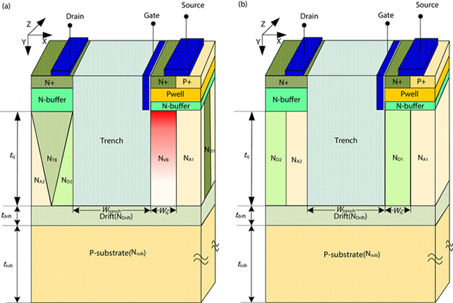
The structure of the DC DT SJ LDMOS is shown asFig. 1(a).tsj,tdrift, andtsub represent the thickness of the SJ, the thickness of the bottom drift region and the thickness of the substrate respectively,Wsj represents the width of the super junction on both sides of the SiO2 dielectric trench, and the width of the compensation layer is equal to the width of the SJ region.Wtrench is the width of the SiO2 dielectric trench.Ndrift andNsub are the doping concentration of the drift region at the bottom of the SiO2 dielectric trench and the doping concentration of the substrate, respectively. The doping concentration of the P–N–P type SJ region under the source is the same,NA1 =ND1 =Nsj. The doping concentration of the triangle-like SJ region under the drain level is the same,NA2 =ND2 =Nsj2. The concentration of the triangular charge compensation layer on the left side of the SiO2 dielectric trench isNTB. The charge compensation layer on the right side of the SiO2 dielectric trench is vertical variable-doped, and the doping concentration gradually decreases from the top to the bottom, which is represented byNVB.
Table Infomation Is Not Enable

Figure 1.(Color online) The structure of (a) DC DT SJ LDMOS and (b) Con. DT SJ LDMOS.
As can seen from theFig. 1(a), the DC DT SJ LDMOS device structure has a triangular charge compensation layer on the left side of the SiO2 dielectric trench. The addition of the triangular charge compensation layer makes the conventional P-pillar and N-pillar SJ structure with equal width and equal concentration become a triangular-like SJ structure. The inverted triangle form of the charge compensation layer fully compensates the charge accumulated by the SIS parallel plate capacitance generated on both sides of the SiO2 dielectric trench. The right-hand side of the SiO2 dielectric trench adopts the P-type charge compensation layer in the form of vertical variable doping. The P-type gradient compensation layer can also fully compensate the charge generated by the SIS capacitor, and the SJ region returns to the charge balance state. The SJ region at the source side of the SiO2 dielectric trench is a P–N–P type SJ structure. The addition of a new voltage-resistant junction improves the BV of the device in both horizontal and vertical directions. The structure of the Con. DT SJ LDMOS is shown inFig. 1(b).
The main parameters of the device structure of DC DT SJ LDMOS are shown inTable 1.
Fig. 2 shows the charge compensation principle of the DC DT SJ LDMOS. The vertical variable-doped P pillar at the source side and the inverted triangular N pillar at the drain side are used to compensate for the vertically distributed charges accumulated on both sides of the trench SiO2 capacitor. The triangular-like SJ structure at the source side and the PNP structure at the drain side can deplete each other and maintain charge balance, so that the device reaches the charge balance.
Figure 2.(Color online) Structure and composition of the DC DT SJ LDMOS.
Compared with the structure of the Con. DT SJ LDMOS device, the problem of charge imbalance due to SIS capacitance can be solved. The P–N–P type SJ structure at the source can modulate the internal electric field of the device.
The BV of DC DT SJ LDMOS has increased by 28.9% to 705.5 V. In the on-state, the current path is widen at the drain, and the doping concentration of triangular-like SJ region at the drain and P–N–P structure source is higher than that of the Con. DT SJ LDMOS so theRon,sp can be reduced significantly.
The vertical variable-doped P-type charge compensation layer provides more uniform and sufficient charge compensation for the charge imbalance in the SJ region caused by the SIS capacitors on both sides of the SiO2 dielectric trench. The change gradient of the vertical concentration of the P-type charge compensation layer is optimized by simulation.
The doping concentration of the P-type charge compensation layer on the right-hand side of the SiO2 dielectric trench changes linearly. The position of the charge compensation layer is 3 to 20μm in they direction, and the thickness is 17μm. The doping concentration gradually decreased from 2 × 10¹⁵ to 1 × 1015 cm−3. The concentration change gradient formula is:
Optimization of the parameters
This section discusses the effects ofND1,NA1,ND2,NA2,Ndrift,NTB andNVB on the BV,Ron,sp and FOM of the DC DT SJ LDMOS device. The above structure parameters were optimized by simulation.
Fig. 3 depicts the variation of the BV of the Con. DT SJ LDMOS and DC DT SJ LDMOS device with theNsj at the source. It can be seen from the figure that the optimal value of the BV of the Con. DT SJ LDMOS is just 549.5 when theNsj is 5 × 1015 cm−3 while the BV of the DC DT SJ LDMOS reaches a maximum of 705.5 V when theNsj is 1.2 × 1016 cm−3. For the DC DT SJ LDMOS, when theNsj ≤ 1.2 × 1016 cm−3, the BV increases with the Nsj. This happens because the electron-hole pairs in the device were not fully depleted and the space charge region formed by the PN junction will form an electric field spike, leading to premature breakdown of the device. After theNsj exceeds the optimal value, the BV decreases with the increase ofNsj, because the excess electrons or holes cannot be completely depleted, the BV begins to drop again.
Figure 3.(Color online) The influence ofNsj at source on BV of Con. DT SJ LDMOS and DC DT SJ LDMOS.
Fig. 4 shows the BV and FOM of the DC DT SJ LDMOS device with the change of the triangle-like SJ doping concentrationNsj2 at the drain side. The two curves of the device show a trend of first rising and then falling. When the concentration ofNsj2 is 7 × 1015 cm−3, the BV and FOM reach the maximum. The reason of this trend is similar toFig. 3, which is related to the depletion of electron-hole pairs.
Figure 4.(Color online) The influence ofNsj2 at the drain on BV of DC DT SJ LDMOS.
Fig. 5 shows the influence ofNTB at the drain side on BV and FOM for the DC DT SJ LDMOS. The N-type region in the triangular SJ will not only deplete part of the charge through the SIS capacitance effect but also deplete with the P-type region. To achieve charge balance, a triangular charge compensation layer under the drain is added to compensate for holes that are not depleted in the P-type SJ region due to the SIS capacitance effect. The optimization of the doping concentrationNTB in the triangular charge compensation layer can better solve the charge imbalance issue caused by the SIS capacitance effect. The compensation layer is an inverted triangle, which is uniformly doped, and the amount of compensation charge gradually decreases from the top to the bottom. Since the SJ region is in charge unbalanced state, which is affected by the SIS capacitance and will result in a decrease in BV.
Figure 5.(Color online) The influence ofNTB at the drain on BV of DC DT SJ LDMOS.
It is very sensitive for BV that the changes in concentration of the charge compensation layer may cause a decay in its value.
It can be seen fromFig. 5 that when the triangular charge compensation layerNTB = 5 × 1015 cm−3, the BV and FOM reached the maximum. Both curves show a trend of increasing first and then decreasing, when the doping concentration increases from 1 × 10¹⁵ to 5 × 1015 cm−3.
Fig. 6 shows how the change of vertical variable charge compensation layer doping concentrationNVB influences BV and FOM. The doping concentration of the vertical variable doped charge compensation layer decreases with the increase ofY, and the doping concentration change is shown as Eq. (1). As shown inFig. 6, whenNVB,min = 1 × 1015 cm−3 andNVB,max = 1 × 1015 cm−3, the BV reaches the maximum. When the BV reaches the optimal value, the maximum concentration of the linear variable doping is 2 × 1015 cm−3. When the concentration of the vertical variable doping region is optimized to the optimum, the problem caused by the SIS capacitance effect in the SJ region is solved, and the SJ region returns to the charge balance state. The BV of DC DT SJ LDMOS device rises. TheRon,sp is not affected by doping concentration. This happens because the current does not flow through the vertical variable doping P pillar. Consequently, when the BV achieves the optimal value, the FOM also achieves the optimal value.
Figure 6.(Color online) The influence ofNVB on BV of DC DT SJ LDMOS. (a) Influence ofNVB, max on BV of DC DT SJ LDMOS. (b) Influence ofNVB,min on BV of DC DT SJ LDMOS.
Fig. 7 shows the influence ofNdrift on the BV and FOM of Con. DT SJ LDMOS and DC DT SJ LDMOS. From the figure it can be seen when the BV reaches the optimal value, theNdrift are 5 × 10¹⁵ and 7 × 1015 cm−3. TheNdrift of DC DT SJ LDMOS is higher than that of Con. DT SJ LDMOS. The N-type drift region at the bottom of the trench is mainly depleted with the P-type substrate to form a vertical P–N junction, which improves the device BV. It also serves as the necessary current path when the device is in the on state.Ndrift also has great influence on theRon,sp. It can be seen from the figure that when theNdrift = 7 × 1015 cm−3, the BV and FOM of the DC DT SJ LDMOS reached the maximum. After the driftNdrift reaches the optimal value, the P-type substrate is completely depleted, the BV of the DC DT SJ LDMOS device reaches the maximum value of 705.5 V.
Figure 7.(Color online) The influence ofNdrift on BV and FOM of Con. DT SJ LDMOS and DC DT SJ LDMOS.
In this part, the optimization process of key parameters that affects the performance of the device we proposed are shown as figures. In addition, the optimal value of each parameter is obtained. Compared with Con. DT SJ LDMOS, the charge imbalance problem of the Con. DT SJ LDMOS is solved by the double charge compensation layer. The electric field is modulated, and a higher BV is obtained. Compared with the Con. DT SJ LDMOS, the concentration of the drift region and SJ region of the new structure has been improved, and the conduction path is widened, which reduces theRon,sp and achieves a much higher FOM.
Results of the simulation
The DC DT SJ LDMOS structure device with a double charge compensation layer is proposed for the problem of trench type SJ SIS capacitor in this paper. This section conducts a targeted study on the BV when the DC DT SJ LDMOS is in the off state and theRon,sp in the on state, and compares the results of simulation to verify the principle of the device structure.
Fig. 8 shows the distribution of equipotential lines when the DC DT SJ LDMOS and Con. DT SJ LDMOS device are in the off state. Compared with the Con DT SJ LDMOS, the equipotential distribution of the new structure is denser, especially at the drain.
Figure 8.(Color online) The distribution of equipotential lines in the off state of (a) Con. DT SJ LDMOS, (b) DC DT SJ LDMOS.
Fig. 9 shows the surface electric field (Y = 0.01μm) and the electric field (Y = 10μm) of the body of the DC DT SJ LDMOS device and Con. DT SJ LDMOS device in the off state. From this figure, it can be seen that the surface electric and both the surface electric field and the bulk electric field of the proposed structure are higher than those of the Con. DT SJ LDMOS. The BV of the proposed structure is also higher than that of the Con. DT SJ LDMOS.
Figure 9.(Color online) The surface electric field (Y = 0.01μm) and the electric field (Y = 10μm) of the SJ region of the DC DT SJ LDMOS device and Con. DT SJ LDMOS device in the off state.
Fig. 10 shows the breakdown characteristic curve of DC DT SJ LDMOS and Con. DT SJ LDMOS in the off state and the output characteristic curve in the on state. It can be seen from the figure that the BV of DC DT SJ LDMOS is 705.5 V, which is higer than 549.5 V of Con. DT SJ LDMOS. The illustration in theFig. 10 shows the output characteristic curves corresponding to the gate voltage 15 V of DC DT SJ LDMOS and the Con. DT SJ LDMOS respectively. It can be seen from this figure that both the on-state and off-state characteristics of the proposed structure are better than those of the Con. DT SJ LDMOS.
Figure 10.(Color online) Measured off-state breakdown curve and on-stateId–Vd curves withVg = 15 V in the illustration of the TCCL DT SJ LDMOS and Con. DT SJ LDMOS.
Fig. 11 shows the relationships between BV andRon,sp for Con. DT SJ LDMOS, some other reported structures[12-18] and DC DT SJ LDMOS proposed in this paper. From the figure it can be seen that the electrical performance of the device breaks through the “silicon limit”[11].
Figure 11.(Color online) TheRon,sp versus BV for different SJ LDMOSTs.
Conclusion
The SIS capacitor of deep trench SJ devices leads to charge imbalance in the SJ region. The DC DT SJ LDMOS is proposed in this paper to solve this problem, which adds a vertical variable doping compensation layer on the source side and an inverted triangular charge compensation layer on the drain based on the Con. DT SJ LDMOS. Moreover, the P–N–P dual voltage-resistant junction technology is used to improve the BV of the device. The double charge compensation layer solves the problem of the charge imbalance of the SJ region caused by the SIS capacitance. The P–N–P dual voltage-resistant junction technology adjusts the internal electric field, so that the BV of the device is improved. In addition, the current path is widen by the triangular-like SJ at the drain.
The simulation results show that compared with the Con. DT SJ LDMOS, the BV increases by 28.9% to 705.5 V, and theRon,sp of the device is reduced by 50.2% to 23.7 mΩ·cm2, and the FOM reached 21.0 MW/cm2.
References
[1] Coe D J. High voltage semiconductor device. United States Patent US 4754310, 1988
[2] Chen X. Semiconductor power devices with alternating conductivity type high-voltage breakdown regions. United States Patent US 5216275, 1993
[3] M Zitouni, F Morancho, P Rossel et al. A new concept for the lateral DMOS transistor for smart power IC's. 11th International Symposium on Power Semiconductor Devices and ICs, 73(1999).
[4] R K Williams, M N Darwish, R A Blanchard et al. The trench power MOSFET: Part I—History, technology, and prospects. IEEE Trans Electron Devices, 64, 674(2017).
[5] L Theolier, H Mahfoz-Kotb, K Isoird et al. A new junction termination using a deep trench filled with BenzoCycloButene. IEEE Electron Device Lett, 30, 687(2009).
[6] C Xia, X H Cheng, Z J Wang et al. Improvement of SOI trench LDMOS performance with double vertical metal field plate. IEEE Trans Electron Devices, 61, 3477(2014).
[7] J Park, K Ko, J Eum et al. A proposal of LDMOS using Deep Trench poly field plate. 2015 IEEE 27th International Symposium on Power Semiconductor Devices & IC's, 149(2015).
[8] Z Cao, B X Duan, T T Shi et al. Theory analyses of SJ-LDMOS with multiple floating buried layers based on bulk electric field modulation. IEEE Trans Electron Devices, 65, 2565(2018).
[9] J J Cheng, P Li, W Z Chen et al. Simulation study of a super-junction deep-trench LDMOS with a trapezoidal trench. IEEE J Electron Devices Soc, 6, 1091(2018).
[10] K Zhou, X R Luo, Z J Li et al. Analytical model and new structure of the variable-k dielectric trench LDMOS with improved breakdown voltage and specific ON-resistance. IEEE Trans Electron Devices, 62, 3334(2015).
[11] D Yang, S D Hu, J M Lei et al. An ultra-low specific on-resistance double-gate trench SOI LDMOS with P/N Pillars. Superlattices Microstruct, 112, 269(2017).
[12] J J Cheng, W Z Chen, P Li. Improvement of deep-trench LDMOS with variation vertical doping for charge-balance super-junction. IEEE Trans Electron Devices, 65, 1404(2018).
[13] M M H Iqbal, F Udrea, E Napoli. On the static performance of the RESURF LDMOSFETS for power ICs. 2009 21st International Symposium on Power Semiconductor Devices & IC's, 247(2009).
[14] B X Duan, S Yuan, Z Cao et al. New superjunction LDMOS with the complete charge compensation by the electric field modulation. IEEE Electron Device Lett, 35, 1115(2014).
[15] Y D Wang, B X Duan, C Zhang et al. AC-SJ VDMOS with ultra-low resistance. Micro Nano Lett, 15, 230(2020).
[16] W T Zhang, R Wang, S K Cheng et al. Optimization and experiments of lateral semi-superjunction device based on normalized current-carrying capability. IEEE Electron Device Lett, 40, 1969(2019).
[17] S Iwamoto, K Takahashi, H Kuribayashi et al. Above 500V class Superjunction MOSFETs fabricated by deep trench etching and epitaxial growth. The 17th International Symposium on Power Semiconductor Devices and ICs, 31(2005).
[18] P Nautiyal, A Agrawal, S Kumari et al. Electrical characteristic investigation of variation vertical doping superjunction UMOS. 2019 IEEE 16th India Council International Conference, 1(2019).
[19] P K Kushwaha, P Nautiyal, A Gupta et al. An improved SJ UMOS with modified gate electrode to reduce gate charge. 2019 9th Annual Information Technology, Electromechanical Engineering and Microelectronics Conference, 81(2019).
[20] L J Wu, Q L Ding, J Q Chen. Improved deep trench super-junction LDMOS breakdown voltage by shielded silicon-insulator-silicon capacitor. Silicon, 13, 3441(2021).
[21] W Z Chen, L J He, Z S Han et al. The simulation study of the SOI trench LDMOS with lateral super junction. IEEE J Electron Devices Soc, 6, 708(2018).