• Photonics Research
  • Vol. 8, Issue 6, 1049 (2020)
Jae Hyeok Lee1、†, Abu Bashar Mohammad Hamidul Islam1、†, Tae Kyoung Kim, Yu-Jung Cha, and Joon Seop Kwak*
Author Affiliations
  • Department of Printed Electronics Engineering, Sunchon National University Jeonnam 540-742, South Korea
  • show less
    DOI: 10.1364/PRJ.385249 Cite this Article Set citation alerts
    Jae Hyeok Lee, Abu Bashar Mohammad Hamidul Islam, Tae Kyoung Kim, Yu-Jung Cha, Joon Seop Kwak. Impact of tin-oxide nanoparticles on improving the carrier transport in the Ag/p-GaN interface of InGaN/GaN micro-light-emitting diodes by originating inhomogeneous Schottky barrier height[J]. Photonics Research, 2020, 8(6): 1049 Copy Citation Text show less
    (a) Schematic diagram of ITO treatment for making L-TLM on a p-GaN surface. (b) Optical microscope image of μ-LED arrays. (c) Schematic fabrication steps of μ-LED arrays.
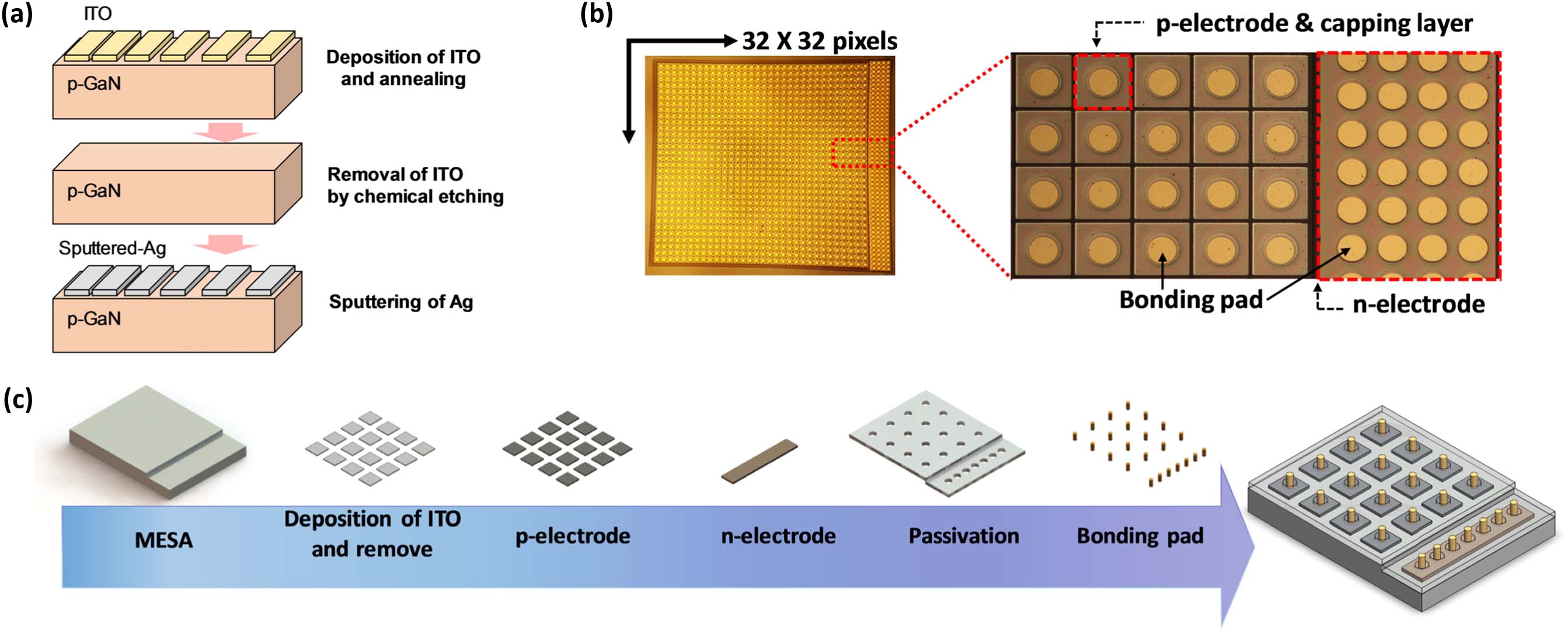
    Fig. 1. (a) Schematic diagram of ITO treatment for making L-TLM on a p-GaN surface. (b) Optical microscope image of μ-LED arrays. (c) Schematic fabrication steps of μ-LED arrays.
    AFM characteristics of p-GaN surface after ITO treatment for ITO thickness of (a) 10, (b) 15, (c) 20, (d) 30, and (e) 60 nm. (f) Surface roughness size, which depends on the ITO thickness.
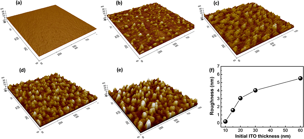
    Fig. 2. AFM characteristics of p-GaN surface after ITO treatment for ITO thickness of (a) 10, (b) 15, (c) 20, (d) 30, and (e) 60 nm. (f) Surface roughness size, which depends on the ITO thickness.
    (a) SEM characteristic after ITO treatment. (b) AES depth profiles according to point 1 and point 2 locations as mentioned in the SEM characteristic. (c) Concentrations of In, Sn, and O as a function of ITO thickness.
    Fig. 3. (a) SEM characteristic after ITO treatment. (b) AES depth profiles according to point 1 and point 2 locations as mentioned in the SEM characteristic. (c) Concentrations of In, Sn, and O as a function of ITO thickness.
    (a) Cross-sectional view of TEM characteristics after ITO treatment of a 30 nm thick ITO layer on a p-GaN surface. EDS profile of (b) In, (c) Sn, and (d) O atoms on a p-GaN surface mentioned in the red dotted box in (a). XPS characteristics of (e) Sn and (f) O particles before and after ITO treatment.
    Fig. 4. (a) Cross-sectional view of TEM characteristics after ITO treatment of a 30 nm thick ITO layer on a p-GaN surface. EDS profile of (b) In, (c) Sn, and (d) O atoms on a p-GaN surface mentioned in the red dotted box in (a). XPS characteristics of (e) Sn and (f) O particles before and after ITO treatment.
    (a) Measured I–V characteristics at a pad spacing of 30 μm for samples without and with ITO treatment. Inset shows the calculated resistance for similar pad spacing. (b) Measured reflectance of Ag/ITO-treatment layer/glass for various kinds of ITO thicknesses. (c) Calculated contact resistivity and measured reflectance (at 450 nm) for various kinds of ITO thicknesses.
    Fig. 5. (a) Measured I–V characteristics at a pad spacing of 30 μm for samples without and with ITO treatment. Inset shows the calculated resistance for similar pad spacing. (b) Measured reflectance of Ag/ITO-treatment layer/glass for various kinds of ITO thicknesses. (c) Calculated contact resistivity and measured reflectance (at 450 nm) for various kinds of ITO thicknesses.
    (a) Temperature-dependent calculated contact resistance by using L-TLM. Temperature-dependent I–V characteristics of (b) 10 and (c) 30 nm thick ITO-treated samples, respectively. (d) Calculated SBH of a 10 nm and a 30 nm thick ITO-treated layer by using the relation between ρcT−1 and 1000/T.
    Fig. 6. (a) Temperature-dependent calculated contact resistance by using L-TLM. Temperature-dependent I–V characteristics of (b) 10 and (c) 30 nm thick ITO-treated samples, respectively. (d) Calculated SBH of a 10 nm and a 30 nm thick ITO-treated layer by using the relation between ρcT1 and 1000/T.
    Formation of inhomogeneous SBH caused by the fabricated SnO nanoparticles at MS contact.
    Fig. 7. Formation of inhomogeneous SBH caused by the fabricated SnO nanoparticles at MS contact.
    (a) I–V characteristics of the μ-LEDs with various kinds of ITO-treated thicknesses. Inset shows the forward voltages from 1 to 16 pixels at 83 A/cm2. (b) LOPs of μ-LEDs at various kinds of ITO-treated thicknesses. Inset shows the LOPs from 1 to 16 pixels at 83 A/cm2. (c) The relationship among contact resistance, reflectance, and Sn concentration of μ-LEDs without and with ITO treatment. (d) Aging effect of 10 nm thick ITO-treated μ-LED at an aging temperature of 85°C, where the LOPs are measured at 83 A/cm2.
    Fig. 8. (a) I–V characteristics of the μ-LEDs with various kinds of ITO-treated thicknesses. Inset shows the forward voltages from 1 to 16 pixels at 83  A/cm2. (b) LOPs of μ-LEDs at various kinds of ITO-treated thicknesses. Inset shows the LOPs from 1 to 16 pixels at 83  A/cm2. (c) The relationship among contact resistance, reflectance, and Sn concentration of μ-LEDs without and with ITO treatment. (d) Aging effect of 10 nm thick ITO-treated μ-LED at an aging temperature of 85°C, where the LOPs are measured at 83  A/cm2.
    (a) Distribution of EL intensity over the chip area and (b) EL intensity of μ-LEDs without and with ITO treatment at 83 A/cm2.
    Fig. 9. (a) Distribution of EL intensity over the chip area and (b) EL intensity of μ-LEDs without and with ITO treatment at 83  A/cm2.
    Jae Hyeok Lee, Abu Bashar Mohammad Hamidul Islam, Tae Kyoung Kim, Yu-Jung Cha, Joon Seop Kwak. Impact of tin-oxide nanoparticles on improving the carrier transport in the Ag/p-GaN interface of InGaN/GaN micro-light-emitting diodes by originating inhomogeneous Schottky barrier height[J]. Photonics Research, 2020, 8(6): 1049
    Download Citation