Abstract
The effect of tin-oxide (SnO) nanoparticles, which are obtained by indium-tin-oxide (ITO) treatment, on the p-GaN surface of GaN-based flip-chip blue micro-light-emitting diode (-LED) arrays is investigated. A thin Ag layer is deposited on the ITO-treated p-GaN surface by sputtering. SnO nanoparticles originate from inhomogeneous Schottky barrier heights (SBHs) at Ag/p-GaN contact. Therefore, effective SBH is reduced, which causes carrier transport into the -LED to enhance. 10 nm thick ITO-treated -LEDs show better optoelectronic characteristics among fabricated -LEDs owing to improved ohmic contact and highly reflective p-type reflectors. Basically, SnO nanoparticles help to make good ohmic contact, which results in improved carrier transport into -LEDs and thus results in increased optoelectronic performances.1. INTRODUCTION
Recently, GaN-based high-power light-emitting diodes (LEDs) have attracted great consideration due to their potential applications in displays, headlamps, solid-state lighting, and indoor and outdoor lamps [1–4]. At driving current, the light-output power (LOP) and the external quantum efficiency (EQE) must be high for these applications [5]. However, the increase in junction temperature in top-emitting LEDs is one of the major issues to reduce the EQE and LOP at driving current [6,7] because the conventional top-emitting LEDs have been using an insulating sapphire substrate, which has poor thermal conductivity. Hence, the excessive generated heat is an unavoidable inherent characteristic of top-emitting LEDs, that causes the junction temperature in these LEDs to increase. As a result, the efficiency is reduced, which hinders the further development of high-power LEDs [8]. Thus, bottom-emitting LEDs, namely, vertical and flip-chip LEDs, have attracted considerable attention for having the ability to enhance both light extraction efficiency (LEE) and LOP as well as having better heat dissipation [9–11] due to being commonly bonded with a high-thermal-conductivity submount (such as copper, silicon, or ceramic) that provides a thermal path for the generated heat. Flip-chip LEDs have relatively higher LEE among top- and bottom-emitting LEDs because of low refractive index difference between sapphire () and air ().
In this regard, the p-type contact of flip-chip LEDs must be ohmic with lower contact resistance and higher reflectance in order to achieve high LOP. Three different types of reflectors, the distributed Bragg reflector (DBR) [12–17], the omnidirectional reflector [18], and the metal-based reflector [19], have been used in LEDs. Recently, dielectric DBRs have been widely used in GaN-based LEDs [12–17]. Silver (Ag) is one of the candidates for a highly reflective reflector in flip-chip LEDs, since it has higher reflectance () at visible spectra [20–22]. The work function of Ag is about 4.35 eV, which is not quite favorable to make good ohmic contact with p-GaN [22]. In order to overcome this problem, a high-work-function-based Ni thin layer () between the p-GaN and Ag has been reported [22–24] for improving the p-type ohmic contact. The annealing treatment of metal is crucial for making good ohmic contact. However, thermal annealing of Ag at high temperature creates agglomeration, which deteriorates both electrical resistivity and optical reflectivity. Thus, both the agglomeration (due to annealing) and the decreased reflectance (owing to insertion of an additional metal layer) are inevitable parts for making good ohmic contact between Ag and p-GaN surfaces, which thus results in hampering the further development of high-LOP-based flip-chip LEDs. Therefore, several kinds of attempts have been proposed for preventing Ag from agglomeration/oxidation in order to obtain Ag-based good ohmic contact and high reflectance with p-GaN: a transparent conductive oxide (TCO) layer [25,26], Ag–metal intermetallic [27], pre-annealed indium tin oxide (ITO) [28], and various kinds of metal compositions such as Ni/Ag [22], Zn-Ni/Ag [29], Ni/Au/Ag [30], Ni/Ag/Ti/Au [31], and Pd/Ag/Au/Ti/Au [32]. Despite the abovementioned intensive efforts, Ag agglomeration has still been found due to surface diffusion of Ag atoms caused by the surface energy, which results in grain boundaries having grooves and hillocks formations and then creates agglomeration [33]. Nevertheless, the formation of ohmic contact to a p-GaN layer by using Ag is still not properly understood. Therefore, it is further necessary to investigate Ag/p-GaN-based ohmic contact for enhancing the LOP of bottom-emitting LEDs.
Although flip-chip LEDs have better LOP and heat dissipation capability compared to top-emitting LEDs, the efficiency droop at high current due to nonuniform current spreading caused by the larger chip size is still one of the essential issues [34,35]. Thus, the current crowding effect at high injection current can be eliminated by optimizing the electrode pattern [36], decreasing the chip size [37], and using the current blocking layer [38]; this results in improved optoelectronic characteristics. Recently, micro-LEDs (-LEDs) have emerged as the next-generation LEDs due to their high power at low driving current and the widespread application of -LED arrays as a light source, especially in adaptive driving beams (ADB)/advanced forward lighting systems (AFS) [4].
Sign up for Photonics Research TOC. Get the latest issue of Photonics Research delivered right to you!Sign up now
In this work, we explain the mechanism of improved ohmic contact at the Ag/p-GaN interface by tin oxide (SnO) nanoparticles. First, ITO is deposited on the p-GaN layer, annealed, and finally removed, which is called the ITO treatment. Ag is then deposited on the ITO-treated p-GaN surface using sputtering. Both contact resistance and reflectance are decreased with the increase in ITO thickness. The ITO treatment creates SnO nanoparticles, which are interactively found by using scanning electron microscopy (SEM), transmission electron microscopy (TEM), atomic force microscopy (AFM), X-ray photoelectron spectroscopy (XPS), auger electron spectroscopy (AES), and energy dispersive spectroscopy (EDS) characteristics. Basically, the SnO nanoparticles create an inhomogeneous Schottky barrier height (SBH) at the Ag/p-GaN interface, which causes the effective SBH to decrease. Therefore, the ohmic contact of the Ag/p-GaN interface is improved. This effect is consistently explained by a proposed schematic diagram. Temperature-dependent current–voltage (I–V) characteristics are used to calculate the effective SBH. Based on various kinds of ITO-treated thicknesses, 1024 pixel flip-chip -LED arrays are fabricated in order to investigate the effect of fabricated SnO nanoparticles at the Ag/p-GaN ohmic contact, which results in improvement of the optoelectronic characteristics of -LEDs.
2. SAMPLE STRUCTURE AND EXPERIMENTS
The similar epitaxial structure blue LED wafers are grown on a c-plane patterned sapphire substrate (PSS) by metal-organic chemical vapor deposition (MOCVD). The epitaxial structure consists of a 30 nm thick GaN buffer layer, a 4 μm thick Si-doped n-type GaN layer (), and a 100 nm thick InGaN/GaN superlattice layer, which were consecutively grown on the substrate. The active multiple-quantum-well (MQW) layer was composed of five pairs of 2.3 nm thick wells separated by the 5 nm thick GaN barriers. A 40 nm thick Mg-doped electron-blocking layer, and finally a 200 nm thick Mg-doped p-GaN layer () were successfully grown on the active layer to finish the device structure. The mesa structure was formed by patterning with photolithography, and then it was etched through inductively coupled plasma-reactive ion etching (ICP-RIE) in order to expose the n-GaN layer as shown in Fig. 1(a). Mesa etching was done by ICP-RIE for 7 min until it reached a depth of about 1 μm to expose the n-GaN layer. During this etching process, dry etching parameters such as ICP power, bias power, working pressure, flow, and flow were 900 W, 100 W, , 35 sccm, and 5 sccm, respectively. After removing the photoresist [with acetone, isopropyl alcohol, and deionized (DI) water], the p-GaN surface was cleaned by , HCl:DI, and buffered oxide etchant (BOE) for removing unwanted particles, remaining Ga atoms, and native oxides, respectively, from the p-GaN surface. The line-transmission length method (L-TLM) patterns were made on the p-GaN surface through photolithography for measuring the I–V characteristics to calculate the contact resistance as shown in Fig. 1(a). Various samples with different kinds of 10, 15, 20, 30, and 60 nm thick ITO (: 90%, : 10%) layers were deposited on the patterned p-GaN surface by an electron-beam evaporator. These samples were then annealed at 600°C in ambient for 1 min by using rapid thermal annealing (RTA). Again, , HCl:DI, ITO etchant [ (25%–35%):HCl (3%–4%): ()], and BOE were used to clean and remove the deposited ITO layer (which is defined as ITO treatment) from the p-GaN surface of a sample. As a result, this process creates SnO nanoparticles on the p-GaN surface. In this research work, the SnO nanoparticles on the p-GaN surface are fabricated by using chemical etching instead of pulsed laser ablation method [39] because chemically etched SnO/Ag p-type reflective electrodes have higher reflectivity and good adaptability to the fabrication process compared to the laser ablation method. RF magnetron sputtering was then used to deposit a 250 nm thick Ag film on the p-GaN surface. In this research work, the highly reflective contact electrode is made by depositing Ag film on the ITO-treated p-GaN surface instead of an Ag film covered by TiW/Pt multiple layers [40,41]. During the deposition of Ag on the ITO-treated surface, the following parameters of Ag sputtering were kept constant: Ag target 2-in. (5.08 cm), RF power 100 W, chamber pressure , and Ar flow 20 sccm. After separately investigating the effect of the size of the SnO nanoparticles on the Ag/p-GaN contact electrode, we fabricated different kinds of -LEDs arrays based on various kinds of contacts without ITO treatment and with 10, 30, and 60 nm thick ITO-treated Ag/p-GaN. A Ni/Al/Ni (100/500/100 nm) layer was deposited on the p-type electrode as a capping layer. The n-type electrode was formed by the Cr/Al/Ni (30/500/100 nm) layer on the exposed n-GaN surface, and finally a Ni/Au/Ni/Au (100/600/100/800 nm) layer was deposited on n-type electrode as a capping layer, which also served as a bonding pad. The size of the bonding pad of -LEDs is about 60 μm. The 1024 pixel -LED arrays with a pixel area of were fabricated as seen in Fig. 1(b), and the fabrication steps for the -LEDs are shown in Fig. 1(c).
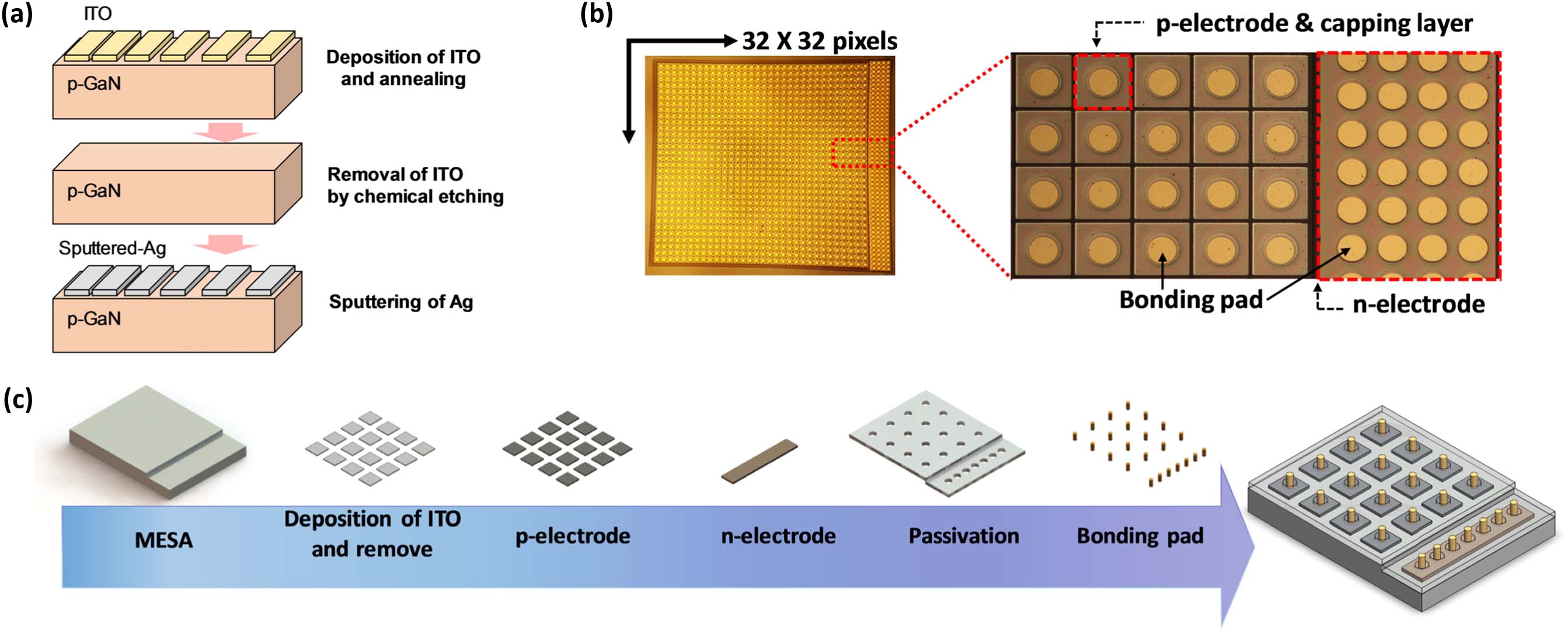
Figure 1.(a) Schematic diagram of ITO treatment for making L-TLM on a p-GaN surface. (b) Optical microscope image of -LED arrays. (c) Schematic fabrication steps of -LED arrays.
The (I–V) characteristics of the samples were measured by a Keithley 4145B source meter with a voltage sweep rate of . A UV/Vis spectroscope (PerkinElmer Lambda 35) was used for measuring the reflectance of samples. A high-resolution charge-coupled-device (CCD) camera was used for recording the two-dimensional electroluminescent (EL) image. A Si p-i-n photodiode was used for measuring the EL intensity. A fiber-optic spectrometer (AvaSpec-2048) was used to record the peak emission wavelength of the -LEDs. An ultrahigh-resolution Schottky field emission SEM (JEOL JSM-7610F Plus) was used for understanding the surface morphology of the -LEDs. An ultrahigh-resolution TEM (Themis Z, Thermo Fisher Scientific) was used for detailed investigation of the ITO-treated p-GaN surface. In addition, an AFM (Park Systems XE-7) was also used for measuring the surface characteristics of the ITO-treated p-GaN surface at the highest nanoscale resolution. The depth profile of ITO-treated surface was measured by an XPS system (Thermo Fisher Scientific, K-Alpha). Both the elemental and chemical states of the ITO-treated surface were scanned by high-performance AES (Physical Electronics, PHI-710).
3. RESULTS AND DISCUSSION
Before investigating all characteristics, the change in p-GaN surface after ITO treatment is observed by using AFM and then SEM (which is not shown in this article) characteristics. The AFM characteristics of thickness varying ITO-treated samples are shown in Figs. 2(a)–2(e). It is found that the ITO treatment causes nanosize roughness on the p-GaN surface. Basically, surface roughness consists of nanoparticles. The average roughness sizes of 10, 15, 20, 30, and 60 nm thick ITO-treated layers on the p-GaN surface are 0.195, 1.592, 3.069, 4.041, and 5.531 nm, respectively, as shown in Fig. 2(f). It indicates that the roughness size on the p-GaN surface is increased with ITO thickness, which is consistently observed by using both AFM and SEM characteristics. The size of roughness on the p-GaN surface is increased because of an increase in nanoparticle density into the roughness area.

Figure 2.AFM characteristics of p-GaN surface after ITO treatment for ITO thickness of (a) 10, (b) 15, (c) 20, (d) 30, and (e) 60 nm. (f) Surface roughness size, which depends on the ITO thickness.
The AES characteristics are taken on the ITO-treated surface for finding the material composition in the roughness. The measured position of AES characteristics is shown in Fig. 3(a), which is taken by using SEM, where point 1 and point 2 represent the measured locations on the surface roughness consisting of nanoparticles and p-GaN surface, respectively. It is found that there are peak amplitudes of Sn and oxygen (O) particles in the point 1 position and gallium (Ga) and nitrogen (N) particles in the point 2 position as shown in Fig. 3(b). At point 1, the AES depth profiles of In, Sn, and O are shown in Fig. 3(c) for different thicknesses of ITO. The depth profile of indium (In) concentration () on the p-GaN surface is almost constant for samples without ITO treatment and ITO-treated samples. On the other hand, the concentrations of Sn and O atoms on the ITO-treated surface have an upward tendency with the increase in ITO thickness. The concentrations of Sn and O are increased about 8.7% and 17%, respectively, as the ITO thickness increased from 0 nm (without ITO) to 60 nm, where those without any ITO layer are assumed to have about 0% of Sn, O, and In particles. These results consistently suggest that the ITO-treated p-GaN surface consists of nanoparticles, which are composed of SnO nanoparticles.
Figure 3.(a) SEM characteristic after ITO treatment. (b) AES depth profiles according to point 1 and point 2 locations as mentioned in the SEM characteristic. (c) Concentrations of In, Sn, and O as a function of ITO thickness.
We have also measured the EDS characteristic to analyze the inside particles of a 30 nm thick ITO-treated sample. The measured EDS cross-section area is shown in Fig. 4(a) with the red dotted box. The EDS analyses of In, Sn, and O atoms into the selected nanoparticles are shown in Figs. 4(b)–4(d), respectively. The In atoms clearly appear inside of the p-GaN layer; however, there is very small amount of In atoms observed on the p-GaN surface. These results also resemble those of the AES characteristics. On the other hand, Sn and O atoms are found in each nanoparticle on the p-GaN surface as seen in Figs. 4(c) and 4(d), respectively. Thus, nanoparticles consist of SnO compounds, which is also consistent with the AES characteristics. In order to confirm the composition of the nanoparticles, XPS characteristics were taken before and after ITO treatment. In the XPS characteristics, the peaks of and are shifted to a higher energy after ITO treatment as shown in Figs. 4(e) and 4(f), respectively. It represents that the Sn atoms have strong bonding with the O atoms, which thus results in forming the SnO nanoparticles. By the analyses of AFM, TEM, AES, EDS, and XPS characteristics, it is consistently found that the ITO treatment creates SnO nanoparticles on the p-GaN surface.
Figure 4.(a) Cross-sectional view of TEM characteristics after ITO treatment of a 30 nm thick ITO layer on a p-GaN surface. EDS profile of (b) In, (c) Sn, and (d) O atoms on a p-GaN surface mentioned in the red dotted box in (a). XPS characteristics of (e) Sn and (f) O particles before and after ITO treatment.
Now, a thin Ag layer is deposited on samples both without and with ITO treatment to investigate the effect of fabricated SnO nanoparticles in between Ag/p-GaN contact. The measured I–V characteristics of samples without ITO treatment and those with various kinds of ITO-treated samples are shown in Fig. 5(a). The sample without ITO treatment suffers from nonlinear I–V characteristics due to the low work function of Ag [22]. However, the I–V characteristics of the ITO-treated samples follow the linear behavior and show a step trend with the increase in ITO thickness. The inset shows the total resistance, which is decreased with the increase in ITO-treated thickness compared to the sample without ITO. Basically, SnO nanoparticles originating from the ITO treatment reduce the effective SBH, which causes the ohmic contact to improve. The measured reflectances of samples without ITO treatment and the 10, 15, 20, 30, and 60 nm thick ITO-treated samples are 100%, 99.7%, 95.6%, 91.5%, 85.0%, and 76.1%, respectively, as shown in Fig. 5(b). The reflectance of a sample is decreased with the increase in ITO thickness (i.e., SnO nanoparticle size). The calculated contact resistance by using L-TLM of samples without ITO treatment and those with 10, 15, 20, 30, and 60 nm thick ITO-treated layers are , , , , , and , seen in Fig. 5(c); these are comparable to the recently reported specific contact resistance of the Ag or ITO contact with the p-GaN layer [40,41]. The contact resistance is decreased with the increase in SnO nanoparticle size on the p-GaN surface [as seen Fig. 2(f)] since the effective SBH at the metal–semiconductor (MS) surface decreases with the ITO-treated thickness. Usually, there is a reflection dip around 300 nm because of the bulk plasma frequency of Ag, which is caused by the d-like valence electron absorption [42]. The reflection dip at about 450 nm is attributed to the excitation of surface plasmon resonance in the grain boundaries [42]. The reflection dip becomes broader and higher with the ITO thickness due to the absorption of light. At 450 nm, the reflectance is decreased with the ITO thickness as found in Fig. 5(c). From these results, it is considered that both contact resistance and reflectance tend to decrease with the ITO-treated thickness, which eventually depends on the size of the fabricated SnO nanoparticles on the p-GaN surface. In addition, it should be noted that the reflectances of samples without any ITO layer (0 nm) and those with a 10 nm thick ITO-treated layer are almost similar; however, the contact resistance of a 10 nm thick ITO-treated sample is significantly lower compared to the sample without ITO because the SnO nanoparticles caused the effective SBH to decrease.
Figure 5.(a) Measured I–V characteristics at a pad spacing of 30 μm for samples without and with ITO treatment. Inset shows the calculated resistance for similar pad spacing. (b) Measured reflectance of Ag/ITO-treatment layer/glass for various kinds of ITO thicknesses. (c) Calculated contact resistivity and measured reflectance (at 450 nm) for various kinds of ITO thicknesses.
Based on temperature, the calculated contact resistances of 10 and 30 nm thick ITO-treated layers by L-TLM measurement are shown in Fig. 6(a); the temperature-dependent I–V characteristics of 10 and 30 nm thick ITO-treated samples are shown in Figs. 6(b) and 6(c), respectively, where the slope of I–V characteristics increases as the temperature increases from 200 to 400 K. The inset shows the calculated sheet resistance. The 30 nm thick ITO-treated sample has lower contact and sheet resistances than the 10 nm thick ITO-treated sample. The decrease in resistance with the increased size of SnO-nanoparticles is because of a decrease in effective SBH. The effective barrier height is estimated by the relationship between the contact resistance and the defect density through the following Eq. (1) [43]: where , , , , and are the Debye temperature, constant, extent of the wave function, defect density, and SBH, respectively [43]. The is calculated from the linear relation between and as seen in Fig. 6(d) for 10 and 30 nm thick ITO-treated layers, which are 0.195 and 0.046 eV, respectively. The difference in calculated SBH between the 10 and the 30 nm thick ITO-treated layers is due to the increased SnO nanoparticles size as already seen in Fig. 2(f). Thus, the intentionally fabricated SnO nanoparticles in between MS contact by using ITO treatment cause the SBH to decrease. Basically, the SnO nanoparticles break the homogeneous SBH at the MS surface. This creates variation of the SBH corresponding to the SnO nanoparticles as explained in Fig. 7. An inhomogeneous SBH at MS contact is formed by a pinch-off effect known as the potential saddle point in the semiconductor [44–49]. As a result, there are many pinch-off-like lower SBHs (blue solid line) surrounded by a higher SBH corresponding to the SnO nanoparticle (red solid line) [44–49]. The difference in SBHs between SnO nanoparticles and MS contact leads to an increase in the electric field at the MS interface [44,45]. Consequently, the barrier height becomes lower due to an increase in electric field [49]. The fabrication of SnO nanoparticles in between the Ag/p-GaN interface reduces the effective SBH (blue solid line), which causes the ohmic contact to improve. Hence, the current density near the lower SBH is higher due to decrease in SBH, which is caused by the SnO nanoparticles, compared to the average current density [50] as seen in Fig. 7, which is consistent with Fig. 5(a). As the roughness size is increased owing to an increase in the size of the fabricated SnO nanoparticles (or ITO thickness), the effective SBH also decreases, which causes the ohmic contact at the MS interface to decrease as seen in Fig. 5. As a result, the carrier transport at the MS surface is enhanced due to fabricated SnO nanoparticles.
Figure 6.(a) Temperature-dependent calculated contact resistance by using L-TLM. Temperature-dependent I–V characteristics of (b) 10 and (c) 30 nm thick ITO-treated samples, respectively. (d) Calculated SBH of a 10 nm and a 30 nm thick ITO-treated layer by using the relation between and .
Figure 7.Formation of inhomogeneous SBH caused by the fabricated SnO nanoparticles at MS contact.
The p-type contact of flip-chip -LED arrays is fabricated according to the investigated method described above to comprehend the effect of Ag/p-GaN contact without and with ITO treatment on the optoelectronic performances. The I–V characteristics of the fabricated -LED arrays based on layers without ITO treatment and with 10, 30, and 60 nm thick ITO-treated layers are shown in Fig. 8(a). At , the measured forward voltages of -LEDs from 1 to 16 pixels are shown in the inset. The calculated average forward voltages of -LEDs without ITO (0 nm) and with 10, 30, and 60 nm thick ITO-treated -LEDs are 4.31, 3.29, 3.17, and 3.20 V, respectively. It is found that the -LEDs without ITO treatment suffer from higher forward voltage because of poor ohmic contact than the fabricated SnO-nanoparticle-based -LEDs. Thus, SnO-nanoparticle-based contact electrodes improve the carrier transport in -LEDs, which causes the forward voltage to decrease. Figure 8(b) shows the LOPs without and with various kinds of thick ITO-treated -LEDs. The inset shows the measured LOPs from 1 to 16 pixels at . The calculated average LOPs are 1.44, 3.27, 2.89, and 2.74 mW for -LEDs without and with 10, 30, and 60 nm thick ITO treatment, respectively. The fabricated SnO-nanoparticle-based -LEDs have higher LOP than those without ITO treatment. In addition, the 10 nm thick ITO-treated -LEDs have the highest LOP among the fabricated -LEDs. To understand the increase in LOP of 10 nm thick ITO-treated -LEDs compared to others, a relationship among fabricated SnO nanoparticles size (the density of Sn), reflectance, and contact resistance is shown in Fig. 8(c). As the ITO treatment thickness is increased, the contact resistance is also decreased owing to the reduced effective SBH, which is caused by the fabricated SnO nanoparticles in between Ag/p-GaN MS contact as already discussed above. However, the increase in contact resistance of a 60 nm thick ITO-treated layer compared to a 30 nm thick ITO-treated layer may be because of the size-dependent saturation effect of SnO nanoparticles fabricated from the thicker ITO-treated layer. The decrease in reflectance is also caused by the increased size of the fabricated SnO nanoparticles with the ITO thickness seen in Fig. 5. On the other hand, a highly reflective p-type reflector is required to improve both the LEE and LOP of flip-chip -LEDs. The fabricated -LEDs both without (0 nm) and with a 10 nm thick ITO-treated layer have similar kind of reflectance (about 100%). However, the increase in LOP of a 10 nm thick ITO-treated -LED among fabricated -LEDs is owing to highly reflective p-type reflector. The -LED without ITO treatment has lower LOP despite having a highly reflective p-type reflector because it has poor contact resistance, which causes bad carrier transport through the p-type electrode as seen in Figs. 5 and 8. The aging effect of a 10 nm thick ITO-treated Ag/p-GaN-based -LED is shown in Fig. 8(d) at a constant aging temperature of about 85°C. It is observed that there is a very small change in forward voltage with the increase in aging time. However, there is no change in LOP during the entire aging time. Therefore, it can be said that there is no issue about the reliability of Ag thin film on the ITO-treated p-GaN surface in GaN-based -LED operation.
Figure 8.(a) I–V characteristics of the -LEDs with various kinds of ITO-treated thicknesses. Inset shows the forward voltages from 1 to 16 pixels at . (b) LOPs of -LEDs at various kinds of ITO-treated thicknesses. Inset shows the LOPs from 1 to 16 pixels at . (c) The relationship among contact resistance, reflectance, and Sn concentration of -LEDs without and with ITO treatment. (d) Aging effect of 10 nm thick ITO-treated -LED at an aging temperature of 85°C, where the LOPs are measured at .
Figure 9(a) shows the EL intensity distribution at for -LEDs without and with 10, 30, and 60 nm thick ITO treatment. It is also found that the SnO-nanoparticle-based -LEDs have uniform light intensity distribution over the chip area compared to the -LED without ITO treatment, since the -LED without ITO treatment has poor contact resistance and carrier transportation. In addition, the 10 nm thick ITO-treated -LED has higher light intensity among fabricated -LEDs, which results from the highly reflective p-type electrode as seen in Figs. 5(c) and 8(b). The EL peak wavelengths of -LEDs without and with ITO treatment are shown in Fig. 9(b). It is also a similar reason for which the 10 nm thick ITO-treated -LED has the higher intensity due to the improved contact resistance and highly reflective p-type reflector. The ITO-treated -LEDs suffer from blue-shift in the peak emission wavelength compared to the -LED without ITO treatment. Usually, surface treatment has no effect on the peak emission wavelength, since -LEDs are fabricated from similar wafers. The emission wavelength depends on the active MQWs. Therefore, the difference in peak emission wavelength between -LEDs without and with ITO treatment may be either due to nonuniform In-composition in the MQWs over the wafer area or fluctuation of potential energy as reported for the blue LEDs fabricated from similar wafers [51].
Figure 9.(a) Distribution of EL intensity over the chip area and (b) EL intensity of -LEDs without and with ITO treatment at .
4. CONCLUSIONS
In summary, we have significantly and interactively investigated the ohmic contact in the Ag/p-GaN MS interface by using no ITO and various kinds of ITO-treated thicknesses. The p-type contact electrode of flip-chip -LED arrays is fabricated without and with SnO nanoparticles to investigate the difference in optoelectronic performances between them. ITO treatment creates SnO nanoparticles on the p-GaN surface, the size of which is increased with the increase in ITO thickness. After ITO treatment, the formation of SnO nanoparticles on p-GaN surface is consistently found by AFM, SEM, TEM, EDS, AES, and XPS characteristics. The difference in SBHs between SnO nanoparticles caused by ITO treatment and MS contact generates inhomogeneous SBH at the MS surface, which causes the effective SBH at the Ag/p-GaN contact to decrease. Both the contact resistance and reflectance of p-type electrode are decreased with the increased size of fabricated SnO nanoparticles in between the Ag/p-GaN interface. The 10 nm thick ITO-treated -LEDs have the highest LOP among the ITO-treated -LEDs since their p-type reflective electrodes have higher reflectance (about 99.7%). At , SnO-nanoparticle-based -LEDs not only have uniform light intensity distribution over the chip area but also higher peak wavelength intensity than the -LED without ITO treatment. In addition, the fabricated SnO-nanoparticle-based -LEDs have lower forward voltage compared to the sample without ITO treatment. Basically, SnO nanoparticles reduce the effective SBH at the MS interface, which causes the contact resistance to decrease and thus results in significantly improved carrier transport into the -LED. Therefore, we anticipate that the intentionally fabricated SnO nanoparticles from the ITO treatment will be a promising fabrication technique to make good Ag/p-GaN-based ohmic contact in order to improve the performance of next-generation flip-chip -LEDs.
References
[1] J. J. Wierer, D. A. Steigerwald, M. R. Krames, J. J. O’shea, M. J. Lu-dowise, G. Christenson, Y.-C. Shen, C. Lowery, P. S. Martin, S. Subramanya, W. Gotz, N. F. Gardner, R. S. Kern, S. A. Stockman. High-power AlGaInN flip-chip light-emitting diodes. Appl. Phys. Lett., 78, 3379-3381(2001).
[2] D. A. Steigerwald, J. C. Bhat, D. Collins, R. M. Fletcher, M. O. Holcomb, M. J. Ludowise, P. S. Martin, S. L. Rudaz. Illumination with solid state lighting technology. IEEE J. Sel. Top. Quantum Electron., 8, 310-320(2002).
[3] C. Weisbuch, M. Piccardo, L. Martinelli, J. Iveland, J. Peretti, J. S. Speck. The efficiency challenge of nitride light-emitting diodes for lighting. Phys. Status Solidi A, 212, 899-913(2015).
[4] S. G. Grötsch, M. Brink, R. Fiederling, T. Liebetrau, I. Möllers, J. Moisel, A. Pfeuffer. “,” SAE Technical Paper 2016-01-1410 ()(2016).
[5] M. H. Crawford. LEDs for solid-state lighting: performance challenges and recent advances. IEEE J. Sel. Top. Quantum Electron., 15, 1028-1040(2009).
[6] J. Piprek. Efficiency droop in nitride-based light-emitting diodes. Phys. Status Solidi A, 207, 2217-2225(2010).
[7] J. Cho, E. F. Schubert, J. K. Kim. Efficiency droop in light-emitting diodes: challenges and countermeasures. Laser Photon. Rev., 7, 408-421(2013).
[8] Y. Zhang, H. Zheng, E. Guo, Y. Cheng, J. Ma, L. Wang, Z. Liu, X. Yi, G. Wang, J. Li. Effects of light extraction efficiency to the efficiency droop of InGaN-based light-emitting diodes. J. Appl. Phys., 113, 014502(2013).
[9] W.-J. Liu, X.-L. Hu, J.-Y. Zhang, G.-E. Weng, X.-Q. Lv, H.-J. Huang, M. Chen, X.-M. Cai, L.-Y. Ying, B.-P. Zhang. Low-temperature bonding technique for fabrication of high-power GaN-based blue vertical light-emitting diodes. Opt. Mater., 34, 1327-1329(2012).
[10] L.-B. Chang, C.-C. Shiue, M.-J. Jeng. Formation process of high reflective Ni/Ag/Au ohmic contact for GaN flip-chip light-emitting diodes. Appl. Phys. Lett., 90, 163515(2007).
[11] L. Yin, Y. Bai, T. Nan, J. Zhang. Performance enhancement of gallium-nitride-based flip-chip light-emitting diode with through-via structure. Phys. Status Solidi A, 212, 1725-1730(2015).
[12] H.-Y. Lin, C.-W. Sher, D.-H. Hsieh, X.-Y. Chen, H.-M. P. Chen, T.-M. Chen, K.-M. Lau, C.-H. Chen, C.-C. Lin, H.-C. Kuo. Optical cross-talk reduction in a quantum dot-based full-color micro-light-emitting-diode display by a lithographic-fabricated photoresist mold. Photon. Res., 5, 411-416(2017).
[13] C.-H. Lin, J.-Y. Tsai, C.-C. Kao, H.-C. Kuo, C.-C. Yu, J.-R. Lo, K.-M. Leung. Enhanced light output in InGaN-based light-emitting diodes with omnidirectional one-dimensional photonic crystals. Jpn. J. Appl. Phys., 45, 1591-1593(2006).
[14] S. Zhou, X. Liu, Y. Gao, Y. Liu, M. Liu, Z. Liu, C. Gui, S. Liu. Numerical and experimental investigation of GaN-based flip-chip light-emitting diodes with highly reflective Ag/TiW and ITO/DBR ohmic contacts. Opt. Express, 25, 26615-26627(2017).
[15] X. Ding, C. Gui, H. Hu, M. Liu, X. Liu, J. Lv, S. Zhou. Reflectance bandwidth and efficiency improvement of light-emitting diodes with double-distributed Bragg reflector. Appl. Opt., 56, 4375-4380(2017).
[16] S. Zhou, C. Zheng, J. Lv, Y. Gao, R. Wang, S. Liu. GaN-based flip-chip LEDs with highly reflective ITO/DBR p-type and via hole-based n-type contacts for enhanced current spreading and light extraction. Opt. Laser Technol., 92, 95-100(2017).
[17] G. J. Lee, I. Y. Hong, T. K. Kim, H. J. Park, S. K. Oh, Y.-J. Cha, M. J. Park, K. J. Choi, J. S. Kwak. Design of ITO/SiO2/TiO2 distributed Bragg reflectors as a p-type electrode in GaN-based flip-chip light emitting diodes. Appl. Surf. Sci., 477, 220-225(2019).
[18] K. H. Lee, Y.-T. Moon, J.-O. Song, J. S. Kwak. Light interaction in sapphire/MgF2/Al triple-layer omnidirectional reflectors in AlGaN-based near ultraviolet light-emitting diodes. Sci. Rep., 5, 9717(2015).
[19] I. Y. Hong, A. B. M. H. Islam, T. K. Kim, Y.-J. Cha, J. S. Kwak. Impact of grain growth of silver reflective electrode by electron bombardment on external quantum efficiency of III-nitride micro-light emitting diode arrays. Appl. Surf. Sci., 512, 145698(2020).
[20] L.-B. Chang, C.-C. Shiue, M.-J. Jeng. High reflective p-GaN/Ni/Ag/Ti/Au ohmic contacts for flip-chip light-emitting diode (FCLED) applications. Appl. Surf. Sci., 255, 6155-6158(2009).
[21] D.-H. Kim, W. C. Lim, J.-S. Park. Highly thermally stable Pd/Zn/Agohmic contact to Ga-face p-type GaN. J. Alloys Compd., 588, 327-331(2014).
[22] H. W. Jang, J.-L. Lee. Mechanism for ohmic contact formation of Ni/Ag contacts on p-type GaN. Appl. Phys. Lett., 85, 5920-5922(2004).
[23] J. H. Son, Y. H. Song, H. K. Yu, J.-L. Lee. Effects of Ni cladding layers on suppression of Ag agglomeration in Ag-based ohmic contacts on p-GaN. Appl. Phys. Lett., 95, 062108(2009).
[24] J. Lv, C. Zheng, Q. Chen, S. Zhou, S. Liu. High power InGaN/GaN flip-chip LEDs with via-hole-based two-level metallization electrodes. Phys. Status Solidi A, 213, 3150-3156(2016).
[25] M. Himmerlich, M. Koufaki, G. Ecke, C. Mauder, V. Cimalla, J. A. Schaefer, A. Kondilis, N. T. Pelekanos, M. Modreanu, S. Krischok, E. Aperathitis. Effect of annealing on the properties of indium–tin–oxynitride films as ohmic contacts for GaN-based optoelectronic devices. ACS Appl. Mater. Interfaces, 1, 1451-1456(2009).
[26] Y. J. Yoon, S. W. Chae, B. K. Kim, M. J. Park, J. S. Kwak. Interfacial reactions of nano-structured Cu-doped indium oxide/indium tin oxide ohmic contacts to p-GaN. J. Nanosci. Nanotechnol., 10, 3254-3259(2010).
[27] Y. H. Song, J. H. Son, H. K. Yu, J. H. Lee, G. H. Jung, J. Y. Lee, J.-L. Lee. Domain matching epitaxy of Mg-containing Ag contact on p-type GaN. Cryst. Growth Des., 11, 2559-2563(2011).
[28] X.-L. Hu, L. Liu, H. Wang, X.-C. Zhang. Effects of pre-annealed ITO film on the electrical characteristics of high-reflectance Ni/Ag/Ni/Au contacts to p-type GaN. Appl. Surf. Sci., 357, 1703-1707(2015).
[29] J.-O. Song, D.-S. Leem, J. S. Kwak, O. H. Nam, Y. Park, T.-Y. Seong. Low-resistance and highly-reflective Zn-Ni solid solution/Ag ohmic contacts for flip-chip light-emitting diodes. Appl. Phys. Lett., 83, 4990-4992(2003).
[30] D. L. Hibbard, S. P. Jung, C. Wang, D. Ullery, Y. S. Zhao, H. P. Lee, W. So, H. Liu. Low resistance high reflectance contacts to p-GaN using oxidized Ni/Au and Al or Ag. Appl. Phys. Lett., 83, 311-313(2003).
[31] R.-M. Lin, Y.-L. Chou, W.-C. Tseng, C.-L. Tsai, J.-C. Li, M.-C. Wu. Thermal stability for reflectance and specific contact resistance of Ni/Ag-based contacts on p-type GaN. Electrochem. Solid-State Lett., 12, H315-H318(2009).
[32] V. Adivarahan, A. Lunev, M. A. Khan, J. Yang, G. Simin, M. S. Shur, R. Gaska. Very-low-specific-resistance Pd/Ag/Au/Ti/Au alloyed ohmic contact to p GaN for high-current devices. Appl. Phys. Lett., 78, 2781-2783(2001).
[33] H. C. Kim, N. D. Theodore, T. L. Alford. Comparison of texture evolution in Ag and Ag(Al) alloy thin films on amorphous SiO2. J. Appl. Phys., 95, 5180-5188(2004).
[34] A. E. Chernyakov, K. A. Bulashevich, S. Y. Karpov, A. L. Zakgeim. Experimental and theoretical study of electrical, thermal, and optical characteristics of InGaN/GaN high-power flip-chip LEDs. Phys. Status Solidi A, 210, 466-469(2013).
[35] D. A. Zakheim, A. S. Pavluchenko, D. A. Bauman, K. A. Bulashevich, O. V. Khokhlev, S. Y. Karpov. Efficiency droop suppression in InGaN-based blue LEDs: experiment and numerical modelling. Phys. Status Solidi A, 209, 456-460(2012).
[36] W. C. Chong, K. M. Lau. Performance enhancements of flip-chip light-emitting diodes with high-density n-type point-contacts. IEEE Electron Device Lett., 35, 1049-1051(2014).
[37] M. S. Wong, D. Hwang, A. I. Alhassan, C. Lee, R. Ley, S. Nakamura, S. P. Denbaars. High efficiency of III-nitride micro-light emitting diodes by sidewall passivation using atomic layer deposition. Opt. Express, 26, 21324-21331(2018).
[38] S. Zhou, S. Yuan, Y. Liu, L. J. Guo, S. Liu, H. Ding. Highly efficient and reliable high power LEDs with patterned sapphire substrate and strip-shaped distributed current blocking layer. Appl. Surf. Sci., 355, 1013-1019(2015).
[39] D.-S. Leem, J.-O. Song, H.-G. Hong, J. S. Kwak, Y. Park, T.-Y. Seong. Low resistance and highly reflective Sb-Doped SnO2/Ag ohmic contacts to p-type GaN for flip-chip LEDs. Electrochem. Solid-State Lett., 7, G219-G221(2004).
[40] S. Zhou, H. Xu, B. Tang, Y. Liu, H. Wan, J. Miao. High-power and reliable GaN-based vertical light-emitting diodes on 4-inch silicon substrate. Opt. Express, 27, A1506-A1516(2019).
[41] S. Zhou, X. Liu, H. Yan, Z. Chen, Y. Liu, S. Liu. Highly efficient GaN-based high-power flip-chip light-emitting diodes. Opt. Express, 27, A669-A692(2019).
[42] S. Auer, W. Wan, X. Huang, A. G. Ramirez, H. Cao. Morphology-induced plasmonic resonances in silver-aluminum alloy thin films. Appl. Phys. Lett., 99, 041116(2011).
[43] J. S. Kwak, O. H. Nam, Y. Park. Temperature-dependent contact resistivity of the nonalloyed ohmic contacts to p-GaN. J. Appl. Phys., 95, 5917-5919(2004).
[44] J. P. Sullivan, R. T. Tung, M. R. Pinto, W. R. Graham. Electron transport of inhomogeneous Schottky barriers: a numerical study. J. Appl. Phys., 70, 7403-7424(1991).
[45] A. Olbrich, J. Vancea, F. Kreupl, H. Hoffmann. Potential pinch-off effect in inhomogeneous Au/Co/GaAs67P33(100)-Schottky contacts. Appl. Phys. Lett., 70, 2559-2561(1997).
[46] A. Olbrich, J. Vancea, F. Kreupl, H. Hoffmann. The origin of the integral barrier height in inhomogeneous Au/Co/GaAs67P33-Schottky contacts: a ballistic electron emission microscopy study. J. Appl. Phys., 83, 358-365(1998).
[47] J. I. Sohn, J.-O. Song, D.-S. Leem, S. Lee, T.-Y. Seong. Nano-dot addition effect on the electrical properties of Ni contacts to p-type GaN. Phys. Status Solidi C, 1, 2524-2527(2004).
[48] J.-O. Song, J. S. Kwak, Y. Park, T.-Y. Seong. Improvement of the light output of InGaN-based light-emitting diodes using Cu-doped indium oxide/indium tin oxide p-type electrodes. Appl. Phys. Lett., 86, 213505(2005).
[49] J.-O. Song, J. S. Kwak, T.-Y. Seong. Improvement of the ohmic characteristics of Pd contacts to p-type GaN using an Ag interlayer. Semicond. Sci. Technol., 21, L7-L10(2005).
[50] R. T. Tung. Electron transport at metal-semiconductor interfaces: general theory. Phys. Rev. B, 45, 13509-13523(1992).
[51] A. B. M. H. Islam, J.-I. Shim, D.-S. Shin. Optoelectronic performance variations in InGaN/GaN multiple-quantum-well light-emitting diodes: effects of potential fluctuation. Materials, 11, 743(2018).

