• Photonics Research
  • Vol. 8, Issue 12, 1958 (2020)
Shihao Sun1, Mingbo He1, Mengyue Xu1, Shengqian Gao1, Ziyan Chen1, Xian Zhang2, Ziliang Ruan2, Xiong Wu3, Lidan Zhou1, Lin Liu1, Chao Lu3, Changjian Guo2, Liu Liu4, Siyuan Yu1, and Xinlun Cai1、*
Author Affiliations
  • 1State Key Laboratory of Optoelectronic Materials and Technologies and School of Electronics and Information Technology, Sun Yat-sen University, Guangzhou 510000, China
  • 2Centre for Optical and Electromagnetic Research, Guangdong Provincial Key Laboratory of Optical Information Materials and Technology, South China Academy of Advanced Optoelectronics, South China Normal University, Higher-Education Mega-Center, Guangzhou, China
  • 3Department of Electronic and Information Engineering, Photonics Research Centre, The Hong Kong Polytechnic University, Hung Hom, Kowloon, Hong Kong, China
  • 4State Key Laboratory for Modern Optical Instrumentation, Centre for Optical and Electromagnetic Research, Zhejiang Provincial Key Laboratory for Sensing Technologies, Zijingang Campus, Zhejiang University, Hangzhou 310058, China
  • show less
    DOI: 10.1364/PRJ.403167 Cite this Article Set citation alerts
    Shihao Sun, Mingbo He, Mengyue Xu, Shengqian Gao, Ziyan Chen, Xian Zhang, Ziliang Ruan, Xiong Wu, Lidan Zhou, Lin Liu, Chao Lu, Changjian Guo, Liu Liu, Siyuan Yu, Xinlun Cai. Bias-drift-free Mach–Zehnder modulators based on a heterogeneous silicon and lithium niobate platform[J]. Photonics Research, 2020, 8(12): 1958 Copy Citation Text show less
    Schematics of the hybrid LN modulator with silicon TOPS. (a) Schematic of the whole structure. The insets are optical mode profiles of modulation and the TOPS region. (b) Perspective view of the TOPS. (c) Cross-section view of the high-speed modulation region and TOPS.
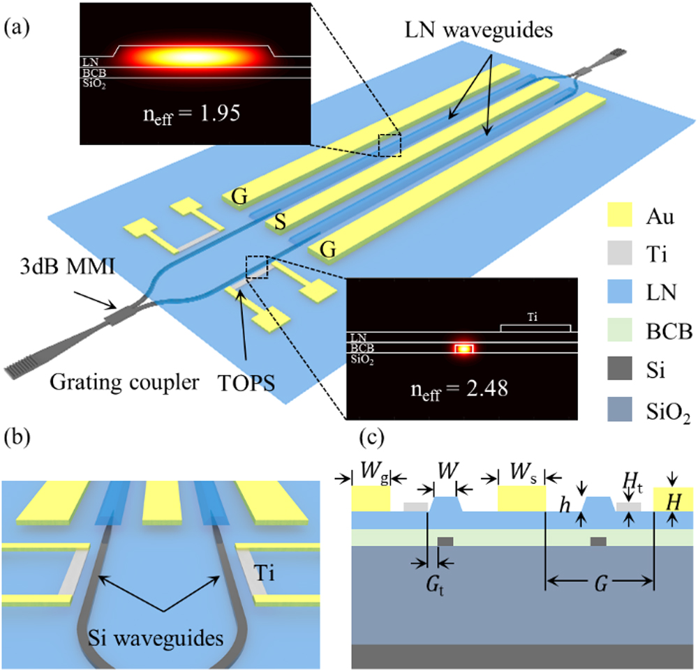
    Fig. 1. Schematics of the hybrid LN modulator with silicon TOPS. (a) Schematic of the whole structure. The insets are optical mode profiles of modulation and the TOPS region. (b) Perspective view of the TOPS. (c) Cross-section view of the high-speed modulation region and TOPS.
    Simulated and experimental results of characteristic impedance Z0, group index ng, and microwave attenuation αm for TWE. The black dashed lines represent the 50 Ω impedance and group index of the optical mode, respectively.
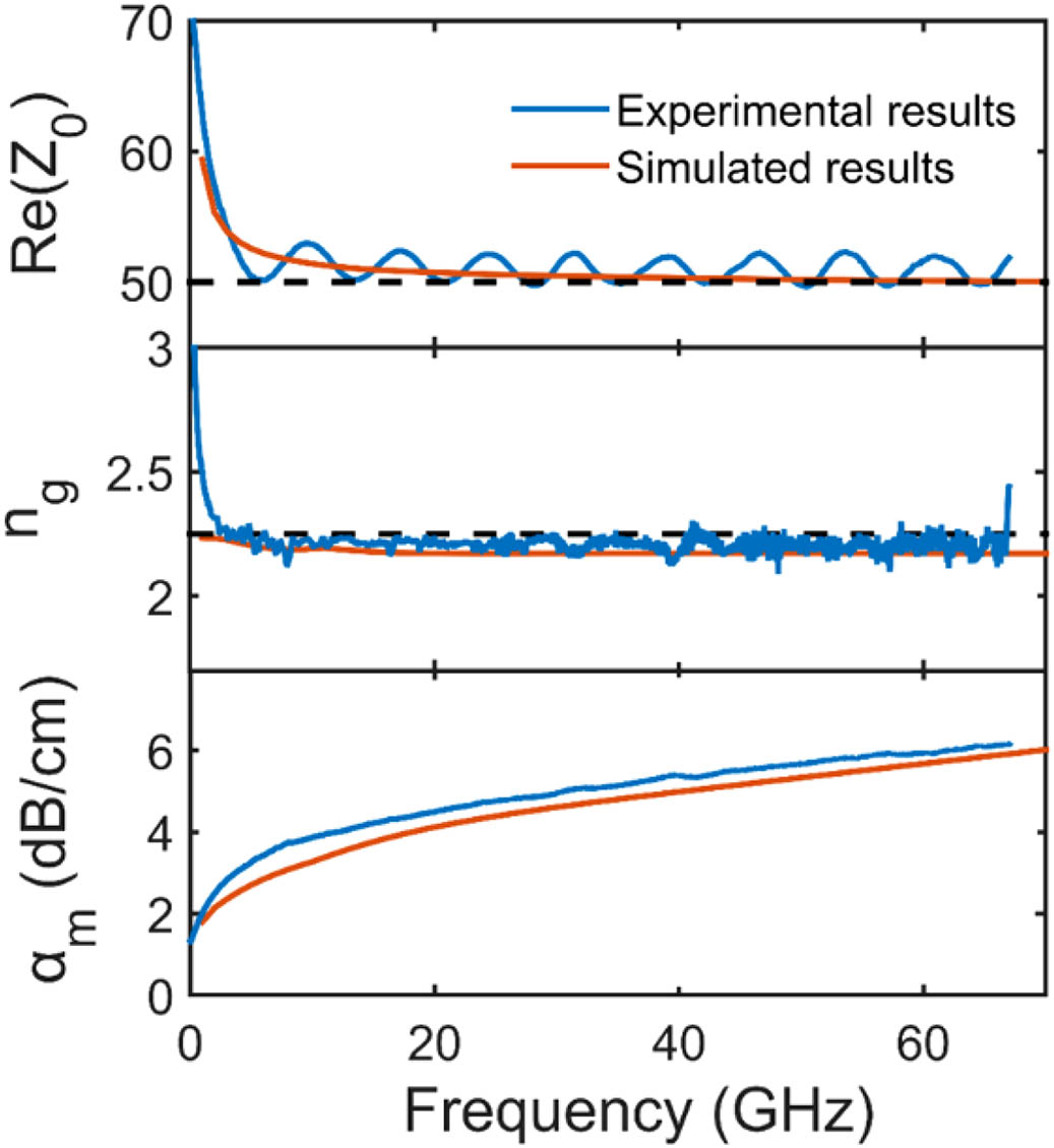
    Fig. 2. Simulated and experimental results of characteristic impedance Z0, group index ng, and microwave attenuation αm for TWE. The black dashed lines represent the 50 Ω impedance and group index of the optical mode, respectively.
    Scanning electron microscopy (SEM) images of the modulator. (a) SEM image of the cross section of the high-speed modulation region. (b) SEM image of the cross section of TOPS. Both sections are formed by the focused ion beam (FIB) process.
    Fig. 3. Scanning electron microscopy (SEM) images of the modulator. (a) SEM image of the cross section of the high-speed modulation region. (b) SEM image of the cross section of TOPS. Both sections are formed by the focused ion beam (FIB) process.
    Experiments of the drift of the operating point for EOPS and TOPS bias control methods. (a) Transmission as a function of applied voltage on TOPS. (b) Power shift for TOPS and EOPS cases as a function of time. (c) Schematic of the experimental setup. The signals from the analog signal generator are set to 10 MHz. (d) Measured SHD intensity variations as a function of time. The red and blue curves correspond to the time-dependence change of SHD for TOPS and EOPS bias control, respectively. (e) Frequency response at the beginning of measurements for both two bias methods. (f), (g) Frequency response for the EOPS and TOPS bias control methods after operating for 2 h, respectively.
    Fig. 4. Experiments of the drift of the operating point for EOPS and TOPS bias control methods. (a) Transmission as a function of applied voltage on TOPS. (b) Power shift for TOPS and EOPS cases as a function of time. (c) Schematic of the experimental setup. The signals from the analog signal generator are set to 10 MHz. (d) Measured SHD intensity variations as a function of time. The red and blue curves correspond to the time-dependence change of SHD for TOPS and EOPS bias control, respectively. (e) Frequency response at the beginning of measurements for both two bias methods. (f), (g) Frequency response for the EOPS and TOPS bias control methods after operating for 2 h, respectively.
    EO performance of hybrid Si and LN modulator. (a) Normalized optical transmissions as a function of the applied voltage on TWE. (b) EO bandwidth (S21 parameter) for the modulator.
    Fig. 5. EO performance of hybrid Si and LN modulator. (a) Normalized optical transmissions as a function of the applied voltage on TWE. (b) EO bandwidth (S21 parameter) for the modulator.
    High-speed transmission experiments. (a), (b) Optical eye diagrams for OOK signal at data rates of 84 Gb/s and 100 Gb/s. (c), (d) Measured PAM-4 modulation optical eye diagrams at 53 Gbaud (106 Gb/s) and 64 Gbaud (128 Gb/s). (e) Measured curves of BER versus the received optical power for 53 Gbaud (106 Gb/s) and 64 Gbaud (128 Gb/s) PAM-4 signals.
    Fig. 6. High-speed transmission experiments. (a), (b) Optical eye diagrams for OOK signal at data rates of 84 Gb/s and 100 Gb/s. (c), (d) Measured PAM-4 modulation optical eye diagrams at 53 Gbaud (106 Gb/s) and 64 Gbaud (128 Gb/s). (e) Measured curves of BER versus the received optical power for 53 Gbaud (106 Gb/s) and 64 Gbaud (128 Gb/s) PAM-4 signals.
    Shihao Sun, Mingbo He, Mengyue Xu, Shengqian Gao, Ziyan Chen, Xian Zhang, Ziliang Ruan, Xiong Wu, Lidan Zhou, Lin Liu, Chao Lu, Changjian Guo, Liu Liu, Siyuan Yu, Xinlun Cai. Bias-drift-free Mach–Zehnder modulators based on a heterogeneous silicon and lithium niobate platform[J]. Photonics Research, 2020, 8(12): 1958
    Download Citation