• Photonics Research
  • Vol. 10, Issue 6, 1401 (2022)
Hao Chen1、†, Zexing Zhao1、†, Ziming Zhang1, Guoqing Wang1, Jiatong Li1, Zhenyuan Shang1, Mengyu Zhang1, Kai Guo2、4、*, Junbo Yang3、5、*, and Peiguang Yan1、6、*
Author Affiliations
  • 1College of Physics and Optoelectronic Engineering, Shenzhen University, Shenzhen 518060, China
  • 2Institute of Systems Engineering, AMS, Beijing 100039, China
  • 3College of Liberal Arts and Sciences, National University of Defense Technology, Changsha 410073, China
  • 4e-mail: guokai07203@hotmail.com
  • 5e-mail: yangjunbo@nudt.edu.cn
  • 6e-mail: yanpg@szu.edu.cn
  • show less
    DOI: 10.1364/PRJ.453520 Cite this Article Set citation alerts
    Hao Chen, Zexing Zhao, Ziming Zhang, Guoqing Wang, Jiatong Li, Zhenyuan Shang, Mengyu Zhang, Kai Guo, Junbo Yang, Peiguang Yan. Heterogeneous integrated phase modulator based on two-dimensional layered materials[J]. Photonics Research, 2022, 10(6): 1401 Copy Citation Text show less
    (a) Schematic of a few-layer MoS2-based phase shifter. The part of the blue dotted square represents the coupling region between the bus waveguide and micro-ring resonator, corresponding to a coupling gap of ∼550 nm. The part of the red dotted square shows the inverse taper waveguide with 350 nm×780 nm cross section and ∼89.4° perpendicularity of the sidewall for a high coupling efficiency. The part of the green dotted square is the active modulation region. The detail illustration is shown in (b), which is the MoS2–SiN integrated structure cladded with ionic liquid (DEME+–TFSI−) to form a capacitor configuration. The bias voltage is used to induce the accumulation of charged carriers at the interface of MoS2 and then change its optical properties.
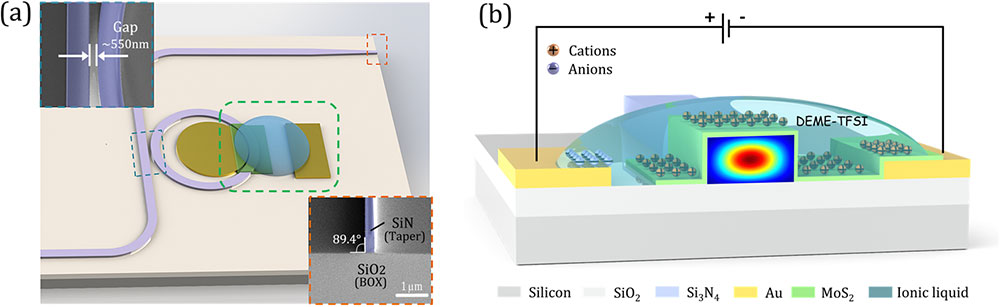
    Fig. 1. (a) Schematic of a few-layer MoS2-based phase shifter. The part of the blue dotted square represents the coupling region between the bus waveguide and micro-ring resonator, corresponding to a coupling gap of 550  nm. The part of the red dotted square shows the inverse taper waveguide with 350  nm×780  nm cross section and 89.4° perpendicularity of the sidewall for a high coupling efficiency. The part of the green dotted square is the active modulation region. The detail illustration is shown in (b), which is the MoS2SiN integrated structure cladded with ionic liquid (DEME+TFSI) to form a capacitor configuration. The bias voltage is used to induce the accumulation of charged carriers at the interface of MoS2 and then change its optical properties.
    (a) Broadband linear absorption spectrum of few-layer MoS2 film. The inset image is the thickness of film measured by an AFM. (b) Raman spectrum of transferred few-layer MoS2, corresponding to the typical Raman vibrational modes.
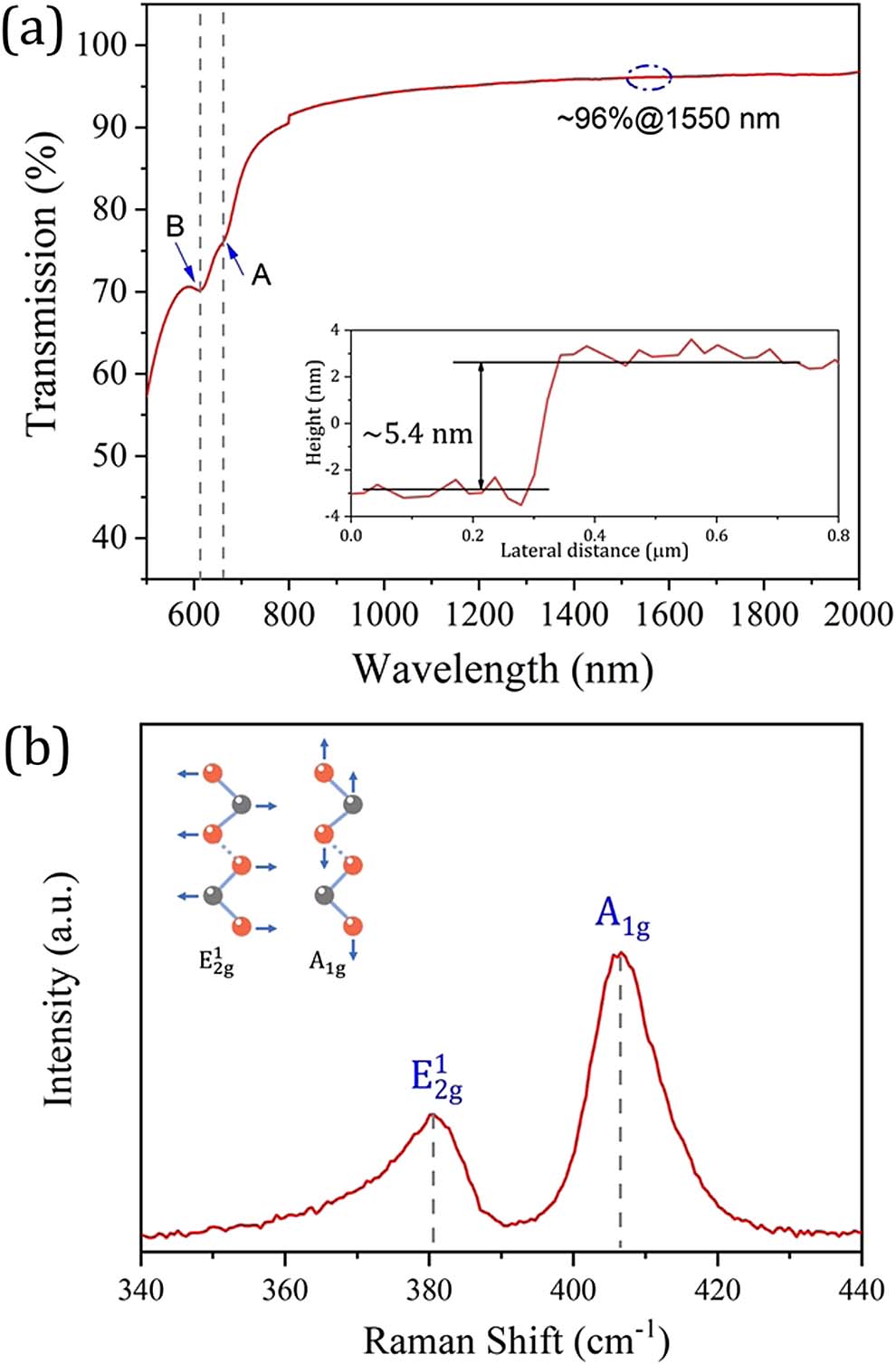
    Fig. 2. (a) Broadband linear absorption spectrum of few-layer MoS2 film. The inset image is the thickness of film measured by an AFM. (b) Raman spectrum of transferred few-layer MoS2, corresponding to the typical Raman vibrational modes.
    (a) Normalized transmission response of the phase shifter as a function of applied bias voltage (cations doping on the interface of MoS2 film). (b) Offset of resonance wavelength, corresponding to a tuning efficiency of 29.42 pm/V. (c) Simulation results of different coupling states for a micro-ring resonator.
    Fig. 3. (a) Normalized transmission response of the phase shifter as a function of applied bias voltage (cations doping on the interface of MoS2 film). (b) Offset of resonance wavelength, corresponding to a tuning efficiency of 29.42 pm/V. (c) Simulation results of different coupling states for a micro-ring resonator.
    (a) Normalized transmission response of a phase shifter as a function of applied bias voltage (anion doping on the surface of MoS2 film). (b) The offset of resonance wavelength at different voltages, which shows a lower tuning efficiency than that of cation doping.
    Fig. 4. (a) Normalized transmission response of a phase shifter as a function of applied bias voltage (anion doping on the surface of MoS2 film). (b) The offset of resonance wavelength at different voltages, which shows a lower tuning efficiency than that of cation doping.
    (a) Normalized transmission response of a phase shifter at high bias voltages. (b) The offset of resonance wavelength loses its linearity at −2.7 V and tends to a similar saturation state when the voltage is further increased.
    Fig. 5. (a) Normalized transmission response of a phase shifter at high bias voltages. (b) The offset of resonance wavelength loses its linearity at 2.7  V and tends to a similar saturation state when the voltage is further increased.
    The effective index of the composite MoS2−SiN waveguide is exacted from the tuned resonance and plotted as a voltage dependent function. The inset images are the energy-band diagram of few-layer MoS2 under different types of charged doping, where EC−N and EV−N are the conduction band edge and valence band edge of n-type MoS2 and EF is the Fermi energy level.
    Fig. 6. The effective index of the composite MoS2SiN waveguide is exacted from the tuned resonance and plotted as a voltage dependent function. The inset images are the energy-band diagram of few-layer MoS2 under different types of charged doping, where ECN and EVN are the conduction band edge and valence band edge of n-type MoS2 and EF is the Fermi energy level.
    PlatformStructureMethodCross Section of WaveguideInsertion Loss (dB)VπL (V·cm)Refs.
    SOIMZMGraphene–silicon480  nm×220  nm/0.28[9]
    SOIMZMLiNbO3–silicon500  nm×220  nm2.52.2[46]
    SOIMZMOrganic–silicon550  nm×220  nm5.41.4[47]
    SOIMZMITO–silicon500  nm×220  nm6.70.0095[48]
    SiNMRRPZT–SiN1000  nm×330  nm/3.3[49]
    SiNRacetrackLiNbO3SiN1200  nm×200  nm135.1[15]
    SiNMZMMoS2SiN1300  nm×330  nm6.61.7[10]
    MRRWS2SiN1300  nm×330  nm/0.8
    SiNMRRMoS2SiN1800  nm×780  nm3.20.69This work
    Table 1. Comparison of Phase Tuning Efficiency for the Hybrid Integrated Phase Modulatora
    Hao Chen, Zexing Zhao, Ziming Zhang, Guoqing Wang, Jiatong Li, Zhenyuan Shang, Mengyu Zhang, Kai Guo, Junbo Yang, Peiguang Yan. Heterogeneous integrated phase modulator based on two-dimensional layered materials[J]. Photonics Research, 2022, 10(6): 1401
    Download Citation