• Opto-Electronic Advances
  • Vol. 5, Issue 8, 210127 (2022)
Svetlana Nikolaevna Khonina1、2、*, Nikolay Lvovich Kazanskiy1、2, Muhammad Ali Butt2、3, and Sergei Vladimirovich Karpeev1、2
Author Affiliations
  • 1IPSI RAS-Branch of the FSRC "Crystallography and Photonics" RAS, Samara 443001, Russia
  • 2Samara National Research University, Samara 443086, Russia
  • 3Warsaw University of Technology, Institute of Microelectronics and Optoelectronics, Koszykowa 75, Warszawa 00-662, Poland
  • show less
    DOI: 10.29026/oea.2022.210127 Cite this Article
    Svetlana Nikolaevna Khonina, Nikolay Lvovich Kazanskiy, Muhammad Ali Butt, Sergei Vladimirovich Karpeev. Optical multiplexing techniques and their marriage for on-chip and optical fiber communication: a review[J]. Opto-Electronic Advances, 2022, 5(8): 210127 Copy Citation Text show less
    The number of research papers associated with different multiplexing techniques indexed in the Scopus database.
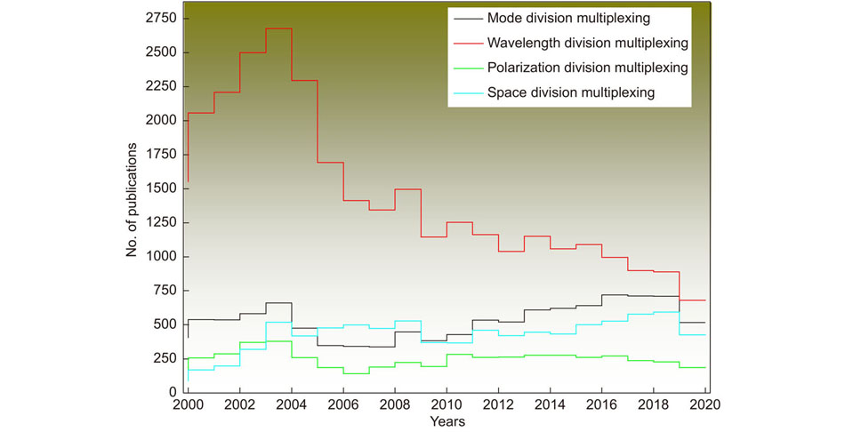
    Fig. 1. The number of research papers associated with different multiplexing techniques indexed in the Scopus database.
    The advancement of transmission volume in FOs established by the state-of-the-art laboratory.
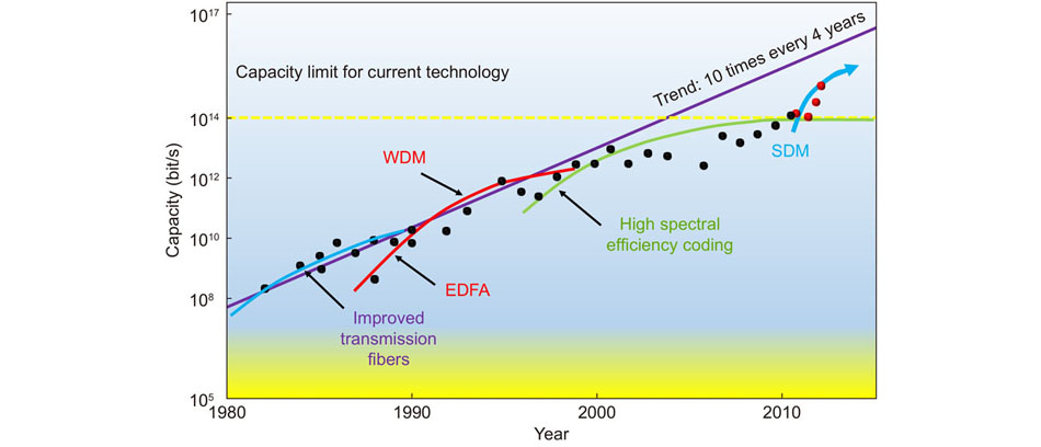
    Fig. 2. The advancement of transmission volume in FOs established by the state-of-the-art laboratory.
    Schematic representation of one-directional WDM broadcast.
    Fig. 3. Schematic representation of one-directional WDM broadcast.
    (a) Graphical illustration of the white-lighting and WDM-VLC network utilizing broadcast gratings and a tailored diffuser over a 20 m FSO link with a 3 m lighting distance. (b) Optical micrographs of the WDM receiver chip. (c) 40 Gbps and 50 Gpbs eye diagrams of channels 5, 10, 15, 20 and 25 at 0 and –1 V. The modulator eye graphs are also displayed for evaluation. Figure reproduced from: (a) ref.35, Optical Society of America; (b) ref.36, Optica Publishing Group, under the Optica Open Access Publishing Agreement.
    Fig. 4. (a) Graphical illustration of the white-lighting and WDM-VLC network utilizing broadcast gratings and a tailored diffuser over a 20 m FSO link with a 3 m lighting distance. (b) Optical micrographs of the WDM receiver chip. (c) 40 Gbps and 50 Gpbs eye diagrams of channels 5, 10, 15, 20 and 25 at 0 and –1 V. The modulator eye graphs are also displayed for evaluation. Figure reproduced from: (a) ref.35, Optical Society of America; (b) ref.36, Optica Publishing Group, under the Optica Open Access Publishing Agreement.
    Schematic representation of the PDM network.
    Fig. 5. Schematic representation of the PDM network.
    4-channel VLC network. Figure reproduced from ref.57, SPIE.
    Fig. 6. 4-channel VLC network. Figure reproduced from ref.57, SPIE.
    The design of an NxN SDM communication network using coherent MIMO digital signal processing. Where MUX/DEMUX represents multiplexer/demultiplexer and Co-Rx signifies Coherent receiver.
    Fig. 7. The design of an NxN SDM communication network using coherent MIMO digital signal processing. Where MUX/DEMUX represents multiplexer/demultiplexer and Co-Rx signifies Coherent receiver.
    Different dissimilarities of FOs for SDM. (a) FO bundle, possibly with compact cladding diameter. (b) Multicore FO with uncoupled cores. (c) Few-mode FO. (d) Coupled-core multicore FO. (e) Multi-mode-multicore FO, in which each core supports more than one mode.
    Fig. 8. Different dissimilarities of FOs for SDM. (a) FO bundle, possibly with compact cladding diameter. (b) Multicore FO with uncoupled cores. (c) Few-mode FO. (d) Coupled-core multicore FO. (e) Multi-mode-multicore FO, in which each core supports more than one mode.
    Effective refractive indices of the guided modes versus width of the core width. Inset shows the mode shapes of the fundamental and higher-order modes. Figure reproduced with permission from ref.88, under a Creative Commons Attribution 4.0 International License.
    Fig. 9. Effective refractive indices of the guided modes versus width of the core width. Inset shows the mode shapes of the fundamental and higher-order modes. Figure reproduced with permission from ref.88, under a Creative Commons Attribution 4.0 International License.
    The operation principle of MDM. The scheme is adapted from ref.90.
    Fig. 10. The operation principle of MDM. The scheme is adapted from ref.90.
    (a) Manufactured TE0 and TE1 mode MUX circuit. (b) SEM images of a manufactured TE0 and TE1 mode (de)MUX and details of its. (c) Input side. (d) Output side91. (e) Graphical representation of a multimode SDM circuit with two polarizations. (f) Schematic of the circuit and structures of (g) μ-RRs-1, (h) μ-RR-2. Figure reproduced from: (a–d) ref.91, Optica Publishing Group, under the Optica Open Access Publishing Agreement; (e) ref.92, Optical Society of America; (f–h) ref.93, Optica Publishing Group, under the Optica Open Access Publishing Agreement.
    Fig. 11. (a) Manufactured TE0 and TE1 mode MUX circuit. (b) SEM images of a manufactured TE0 and TE1 mode (de)MUX and details of its. (c) Input side. (d) Output side91. (e) Graphical representation of a multimode SDM circuit with two polarizations. (f) Schematic of the circuit and structures of (g) μ-RRs-1, (h) μ-RR-2. Figure reproduced from: (a–d) ref.91, Optica Publishing Group, under the Optica Open Access Publishing Agreement; (e) ref.92, Optical Society of America; (f–h) ref.93, Optica Publishing Group, under the Optica Open Access Publishing Agreement.
    (a) Formation of OAM modes with a UCA. (b) Separation of OAM modes with a UCA.
    Fig. 12. (a) Formation of OAM modes with a UCA. (b) Separation of OAM modes with a UCA.
    Hybrid MUX/DEMUX techniques combing multiple individual methods.
    Fig. 13. Hybrid MUX/DEMUX techniques combing multiple individual methods.
    (a) Graphical pattern of the hybrid MUX/DEMUX containing a bi-directional AWG and a polarization diversity circuit. (b) The magnified image of the PDC joining the two input WGs of the bi-directional AWG. Figure reproduced with permission from ref.104, Optica Publishing Group, under the Optica Open Access Publishing Agreement.
    Fig. 14. (a) Graphical pattern of the hybrid MUX/DEMUX containing a bi-directional AWG and a polarization diversity circuit. (b) The magnified image of the PDC joining the two input WGs of the bi-directional AWG. Figure reproduced with permission from ref.104, Optica Publishing Group, under the Optica Open Access Publishing Agreement.
    (a) Schematic representation of a silicon hybrid de (multiplexer) for MDM and WDM. (b) SEM image of the manufactured SiN hybrid MDM-WDM device. SEM pictures of the coupling regions between the input WGs and the bus WGs with a designed bus WG width of, (c) 1 μm, (d) 2.25 μm, (e) 3.5 μm. (f) Schematic representation of a hybrid WDM-MDM MUX/DEMUX. Figure reproduced from: (a) ref.124, (b–e)125, Optica Publishing Group, under the Optica Open Access Publishing Agreement; (f) ref.126, Optical Society of America.
    Fig. 15. (a) Schematic representation of a silicon hybrid de (multiplexer) for MDM and WDM. (b) SEM image of the manufactured SiN hybrid MDM-WDM device. SEM pictures of the coupling regions between the input WGs and the bus WGs with a designed bus WG width of, (c) 1 μm, (d) 2.25 μm, (e) 3.5 μm. (f) Schematic representation of a hybrid WDM-MDM MUX/DEMUX. Figure reproduced from: (a) ref.124, (b–e)125, Optica Publishing Group, under the Optica Open Access Publishing Agreement; (f) ref.126, Optical Society of America.
    Graphical illustration of 10-mode hybrid MUX/DEMUX device for both TE and TM polarizations. Figure reproduced with permission from ref.13, under a Creative Commons Attribution 4.0 InternationalLicense.
    Fig. 16. Graphical illustration of 10-mode hybrid MUX/DEMUX device for both TE and TM polarizations. Figure reproduced with permission from ref.13, under a Creative Commons Attribution 4.0 InternationalLicense.
    Multimode Laguerre-Gauss beams. (a) The DOE phase. (b) The squared modulus of the coefficients in the superposition. (c) The intensity distributions in the focal plane for 5-modes beam (the upper row) and the 6-modes beam (the bottom row). Figure reproduced from ref.154, American Institute of Physics.
    Fig. 17. Multimode Laguerre-Gauss beams. (a) The DOE phase. (b) The squared modulus of the coefficients in the superposition. (c) The intensity distributions in the focal plane for 5-modes beam (the upper row) and the 6-modes beam (the bottom row). Figure reproduced from ref.154, American Institute of Physics.
    Propagation of LP modes superposition in a weakly guiding stepped-index FO (the intensity distribution is taken at different distances z) for (p, q)=(1, 2)+(–2, 1) (top row), (p, q)=(3, 2)+(5, 1) (middle row), (p, q)=(4, 1)+(5, 1) (bottom row). Figure reproduced from ref.189, Pleiades Publishing.
    Fig. 18. Propagation of LP modes superposition in a weakly guiding stepped-index FO (the intensity distribution is taken at different distances z) for (p, q)=(1, 2)+(–2, 1) (top row), (p, q)=(3, 2)+(5, 1) (middle row), (p, q)=(4, 1)+(5, 1) (bottom row). Figure reproduced from ref.189, Pleiades Publishing.
    Instantaneous recognition of particular vortex positions of Laguerre–Gaussian beams. (a) The correlation network with a multi-channel DOE. (b) Results of detection (correlation peaks circled in red) in the focal plane. Figure reproduced from ref.192, under a Creative Commons Attribution.
    Fig. 19. Instantaneous recognition of particular vortex positions of Laguerre–Gaussian beams. (a) The correlation network with a multi-channel DOE. (b) Results of detection (correlation peaks circled in red) in the focal plane. Figure reproduced from ref.192, under a Creative Commons Attribution.
    Binary 14-channel DOE for investigating the polarization and phase positions of vortex cylindrically polarized beams. (a) DOE phase. (b) Correspondence of the diffraction orders in the focal plane to the orders of optical vortices198.
    Fig. 20. Binary 14-channel DOE for investigating the polarization and phase positions of vortex cylindrically polarized beams. (a) DOE phase. (b) Correspondence of the diffraction orders in the focal plane to the orders of optical vortices198.
    (a) The binary phase of the encoded 64-order DOE, matched with LP modes of a step-index FO. (b) The experimentally recorded intensity distribution in the focal plane of the lens when the DOE is illuminated by a plane wave. (c) The arrangement of LP-modes indices p=0,11¯,q=1,5¯ (the conjugate modes with indicesp=−11,0¯ are located symmetrically in the lower part). Figure reproduced with permission from ref.156, under a Creative Commons Attribution 4.0 International License.
    Fig. 21. (a) The binary phase of the encoded 64-order DOE, matched with LP modes of a step-index FO. (b) The experimentally recorded intensity distribution in the focal plane of the lens when the DOE is illuminated by a plane wave. (c) The arrangement of LP-modes indices p=0,11¯, q=1,5¯ (the conjugate modes with indices p=11,0¯ are located symmetrically in the lower part). Figure reproduced with permission from ref.156, under a Creative Commons Attribution 4.0 International License.
    RefYearIL (dB)CT (dB)BW (nm)/∆λch (nm)MT
    ref.1402020<4–9.570MDM
    ref.14120200.08, 0.19, 0.032075MDM
    ref.1422020<0.5–2080MDM
    ref.1432020<1.1–18120MDM
    ref.1442013<1.5<–9100MDM
    ref.1452013~0.3<–36100MDM
    ref.9120130.3–16100MDM
    ref.14620211.61090Hybrid PDM-MDM
    ref.1472021–49.93 to –45.8164–310WDM
    ref.14820180.32–3090MDM
    ref.1492020–23260MDM
    ref.1502019–25140CWDM
    ref.15120140.6–2235Hybrid MDM-WDM
    ref.10420157–133.2Hybrid WDM-PDM
    ref.15220161<-223Hybrid WDM-MDM
    ref.4720180.5–5.0–16.53.2Hybrid WDM-MDM
    Table 1. Few major optical multiplexing papers reported in recent times. IL: Insertion loss, CT: Crosstalk, BW: Bandwidth, MT: Multiplexing technique.
    Svetlana Nikolaevna Khonina, Nikolay Lvovich Kazanskiy, Muhammad Ali Butt, Sergei Vladimirovich Karpeev. Optical multiplexing techniques and their marriage for on-chip and optical fiber communication: a review[J]. Opto-Electronic Advances, 2022, 5(8): 210127
    Download Citation