Journals >Opto-Electronic Advances
Contents


2022
Volume: 5 Issue 8
5 Article(s)
Export citation format
Research Articles
Polarization-switchable plasmonic emitters based on laser-induced bubbles
Jianjun Chen, and Fengyuan Gan
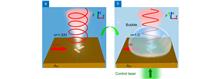
Owing to weak light-matter interactions in natural materials, it is difficult to dynamically tune and switch emission polarization states of plasmonic emitters (or antennas) at nanometer scales. Here, by using a control laser beam to induce a bubble (n=1.0) in water (n=1.333) to obtain a large index variation as high aOwing to weak light-matter interactions in natural materials, it is difficult to dynamically tune and switch emission polarization states of plasmonic emitters (or antennas) at nanometer scales. Here, by using a control laser beam to induce a bubble (n=1.0) in water (n=1.333) to obtain a large index variation as high as |Δn|=0.333, the emission polarization of an ultra-small plasmonic emitter (~0.4λ2) is experimentally switched at nanometer scales. The plasmonic emitter consists of two orthogonal subwavelength metallic nanogroove antennas on a metal surface, and the separation of the two antennas is only sx=120 nm. The emission polarization state of the plasmonic emitter is related to the phase difference between the emission light from the two antennas. Because of a large refractive index variation (|Δn|=0.333), the phase difference is greatly changed when a microbubble emerges in water under a low-intensity control laser. As a result, the emission polarization of the ultra-small plasmonic emitter is dynamically switched from an elliptical polarization state to a linear polarization state, and the change of the degree of linear polarization is as high as Δγ≈0.66. Owing to weak light-matter interactions in natural materials, it is difficult to dynamically tune and switch emission polarization states of plasmonic emitters (or antennas) at nanometer scales. Here, by using a control laser beam to induce a bubble (n=1.0) in water (n=1.333) to obtain a large index variation as high as |Δn|=0.333, the emission polarization of an ultra-small plasmonic emitter (~0.4λ2) is experimentally switched at nanometer scales. The plasmonic emitter consists of two orthogonal subwavelength metallic nanogroove antennas on a metal surface, and the separation of the two antennas is only sx=120 nm. The emission polarization state of the plasmonic emitter is related to the phase difference between the emission light from the two antennas. Because of a large refractive index variation (|Δn|=0.333), the phase difference is greatly changed when a microbubble emerges in water under a low-intensity control laser. As a result, the emission polarization of the ultra-small plasmonic emitter is dynamically switched from an elliptical polarization state to a linear polarization state, and the change of the degree of linear polarization is as high as Δγ≈0.66..
Opto-Electronic Advances
- Publication Date: Aug. 25, 2022
- Vol. 5, Issue 8, 200100 (2022)


Piezoresistive design for electronic skin: from fundamental to emerging applications
Fang Zhong, Wei Hu, Peining Zhu, Han Wang, Chao Ma, Nan Lin, and Zuyong Wang
There is growing recognition that the developments in piezoresistive devices from personal healthcare to artificial intelligence, will emerge as de novo translational success in electronic skin. Here, we review the updates with regard to piezoresistive sensors including basic fundamentals, design and fabrication, and dThere is growing recognition that the developments in piezoresistive devices from personal healthcare to artificial intelligence, will emerge as de novo translational success in electronic skin. Here, we review the updates with regard to piezoresistive sensors including basic fundamentals, design and fabrication, and device performance. We also discuss the prosperous advances in piezoresistive sensor application, which offer perspectives for future electronic skin. There is growing recognition that the developments in piezoresistive devices from personal healthcare to artificial intelligence, will emerge as de novo translational success in electronic skin. Here, we review the updates with regard to piezoresistive sensors including basic fundamentals, design and fabrication, and device performance. We also discuss the prosperous advances in piezoresistive sensor application, which offer perspectives for future electronic skin..
Opto-Electronic Advances
- Publication Date: Aug. 25, 2022
- Vol. 5, Issue 8, 210029 (2022)
Active odd-mode-metachannel for single-conductor systems
Pei Hang He, Ling Yun Niu, Yi Fan, Hao Chi Zhang, Le Peng Zhang, Dayue Yao, Wen Xuan Tang, and Tie Jun Cui
Although tremendous efforts have been devoted to investigating planar single-conductor circuits, it remains challenging to provide tight confinement of electromagnetic field and compatibility with active semi-conductor components such as amplifier, harmonic generator and mixers. Single-conductor spoof surface plasmon pAlthough tremendous efforts have been devoted to investigating planar single-conductor circuits, it remains challenging to provide tight confinement of electromagnetic field and compatibility with active semi-conductor components such as amplifier, harmonic generator and mixers. Single-conductor spoof surface plasmon polariton (SSPP) structure, which is one of the most promising planar single-conductor transmission media due to the outstanding field confinement, still suffers from the difficulty in integrating with the active semi-conductor components. In this paper, a new kind of odd-mode-metachannel (OMM) that can support odd-mode SSPPs is proposed to perform as the fundamental transmission channel of the single-conductor systems. By introducing zigzag decoration, the OMM can strengthen the field confinement and broaden the bandwidth of odd-mode SSPPs simultaneously. More importantly, the active semi-conductor amplifier chip integration is achieved by utilizing the intrinsic potential difference on OMM, which breaks the major obstacle in implementing the single-conductor systems. As an instance, an amplifier is successfully integrated on the single-conductor OMM, which can realize both loss compensation and signal amplification. Meanwhile, the merits of OMM including crosstalk suppression, low radar cross section (RCS), and flexibility are comprehensively demonstrated. Hence, the proposed OMM and its capability to integrate with the active semi-conductor components may provide a new avenue to future single-conductor conformal systems and smart skins.Although tremendous efforts have been devoted to investigating planar single-conductor circuits, it remains challenging to provide tight confinement of electromagnetic field and compatibility with active semi-conductor components such as amplifier, harmonic generator and mixers. Single-conductor spoof surface plasmon polariton (SSPP) structure, which is one of the most promising planar single-conductor transmission media due to the outstanding field confinement, still suffers from the difficulty in integrating with the active semi-conductor components. In this paper, a new kind of odd-mode-metachannel (OMM) that can support odd-mode SSPPs is proposed to perform as the fundamental transmission channel of the single-conductor systems. By introducing zigzag decoration, the OMM can strengthen the field confinement and broaden the bandwidth of odd-mode SSPPs simultaneously. More importantly, the active semi-conductor amplifier chip integration is achieved by utilizing the intrinsic potential difference on OMM, which breaks the major obstacle in implementing the single-conductor systems. As an instance, an amplifier is successfully integrated on the single-conductor OMM, which can realize both loss compensation and signal amplification. Meanwhile, the merits of OMM including crosstalk suppression, low radar cross section (RCS), and flexibility are comprehensively demonstrated. Hence, the proposed OMM and its capability to integrate with the active semi-conductor components may provide a new avenue to future single-conductor conformal systems and smart skins..
Opto-Electronic Advances
- Publication Date: Aug. 25, 2022
- Vol. 5, Issue 8, 210119 (2022)
Optical multiplexing techniques and their marriage for on-chip and optical fiber communication: a review
Svetlana Nikolaevna Khonina, Nikolay Lvovich Kazanskiy, Muhammad Ali Butt, and Sergei Vladimirovich Karpeev
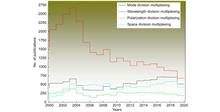
Herein, an attention-grabbing and up-to-date review related to major multiplexing techniques is presented which includes wavelength division multiplexing (WDM), polarization division multiplexing (PDM), space division multiplexing (SDM), mode division multiplexing (MDM) and orbital angular momentum multiplexing (OAMM).Herein, an attention-grabbing and up-to-date review related to major multiplexing techniques is presented which includes wavelength division multiplexing (WDM), polarization division multiplexing (PDM), space division multiplexing (SDM), mode division multiplexing (MDM) and orbital angular momentum multiplexing (OAMM). Multiplexing is a mechanism by which multiple signals are combined into a shared channel used to showcase the maximum capacity of the optical links. However, it is critical to develop hybrid multiplexing methods to allow enhanced channel numbers. In this review, we have also included hybrid multiplexing techniques such as WDM-PDM, WDM-MDM and PDM-MDM. It is probable to attain N×M channels by utilizing N wavelengths and M guided-modes by simply utilizing hybrid WDM-MDM (de)multiplexers. To the best of our knowledge, this review paper is one of its kind which has highlighted the most prominent and recent signs of progress in multiplexing techniques in one place. Herein, an attention-grabbing and up-to-date review related to major multiplexing techniques is presented which includes wavelength division multiplexing (WDM), polarization division multiplexing (PDM), space division multiplexing (SDM), mode division multiplexing (MDM) and orbital angular momentum multiplexing (OAMM). Multiplexing is a mechanism by which multiple signals are combined into a shared channel used to showcase the maximum capacity of the optical links. However, it is critical to develop hybrid multiplexing methods to allow enhanced channel numbers. In this review, we have also included hybrid multiplexing techniques such as WDM-PDM, WDM-MDM and PDM-MDM. It is probable to attain N×M channels by utilizing N wavelengths and M guided-modes by simply utilizing hybrid WDM-MDM (de)multiplexers. To the best of our knowledge, this review paper is one of its kind which has highlighted the most prominent and recent signs of progress in multiplexing techniques in one place..
Opto-Electronic Advances
- Publication Date: Aug. 25, 2022
- Vol. 5, Issue 8, 210127 (2022)
Recent advances in soft electronic materials for intrinsically stretchable optoelectronic systems
Ja Hoon Koo, Huiwon Yun, Woongchan Lee, Sung-Hyuk Sunwoo, Hyung Joon Shim, and Dae-Hyeong Kim
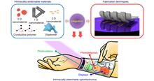
In recent years, significant progress has been achieved in the design and fabrication of stretchable optoelectronic devices. In general, stretchability has been achieved through geometrical modifications of device components, such as with serpentine interconnects or buckled substrates. However, the local stiffness of iIn recent years, significant progress has been achieved in the design and fabrication of stretchable optoelectronic devices. In general, stretchability has been achieved through geometrical modifications of device components, such as with serpentine interconnects or buckled substrates. However, the local stiffness of individual pixels and the limited pixel density of the array have impeded further advancements in stretchable optoelectronics. Therefore, intrinsically stretchable optoelectronics have been proposed as an alternative approach. Herein, we review the recent advances in soft electronic materials for application in intrinsically stretchable optoelectronic devices. First, we introduce various intrinsically stretchable electronic materials, comprised of electronic fillers, elastomers, and surfactants, and exemplify different intrinsically stretchable conducting and semiconducting composites. We also describe the processing methods used to fabricate the electrodes, interconnections, charge transport layers, and optically active layers used in intrinsically stretchable optoelectronic devices. Subsequently, we review representative examples of intrinsically stretchable optoelectronic devices, including light-emitting capacitors, light-emitting diodes, photodetectors, and photovoltaics. Finally, we briefly discuss intrinsically stretchable integrated optoelectronic systems.In recent years, significant progress has been achieved in the design and fabrication of stretchable optoelectronic devices. In general, stretchability has been achieved through geometrical modifications of device components, such as with serpentine interconnects or buckled substrates. However, the local stiffness of individual pixels and the limited pixel density of the array have impeded further advancements in stretchable optoelectronics. Therefore, intrinsically stretchable optoelectronics have been proposed as an alternative approach. Herein, we review the recent advances in soft electronic materials for application in intrinsically stretchable optoelectronic devices. First, we introduce various intrinsically stretchable electronic materials, comprised of electronic fillers, elastomers, and surfactants, and exemplify different intrinsically stretchable conducting and semiconducting composites. We also describe the processing methods used to fabricate the electrodes, interconnections, charge transport layers, and optically active layers used in intrinsically stretchable optoelectronic devices. Subsequently, we review representative examples of intrinsically stretchable optoelectronic devices, including light-emitting capacitors, light-emitting diodes, photodetectors, and photovoltaics. Finally, we briefly discuss intrinsically stretchable integrated optoelectronic systems..
Opto-Electronic Advances
- Publication Date: Aug. 25, 2022
- Vol. 5, Issue 8, 210131 (2022)
© Copyright 2018-2021 | Chinese Laser Press. All Rights Reserved 沪ICP备15018463号-20