• Journal of Semiconductors
  • Vol. 41, Issue 6, 061401 (2020)
Namrata Mendiratta and Suman Lata Tripathi
Author Affiliations
  • School of Electronics and Electrical Engineering, Lovely Professional University, Phagwara, Punjab, India
  • show less
    DOI: 10.1088/1674-4926/41/6/061401 Cite this Article
    Namrata Mendiratta, Suman Lata Tripathi. A review on performance comparison of advanced MOSFET structures below 45 nm technology node[J]. Journal of Semiconductors, 2020, 41(6): 061401 Copy Citation Text show less
    TM-DG MOSFET structure.
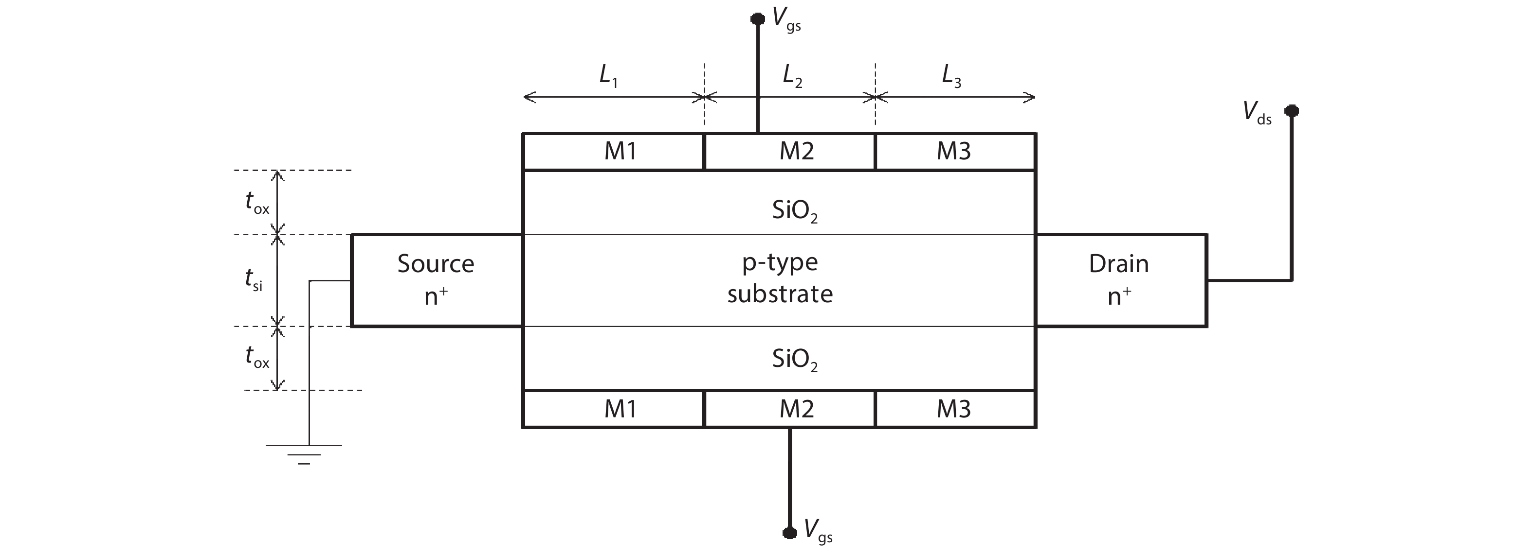
    Fig. 1. TM-DG MOSFET structure.
    GAAJ MOSFET with S/D extensions regions.
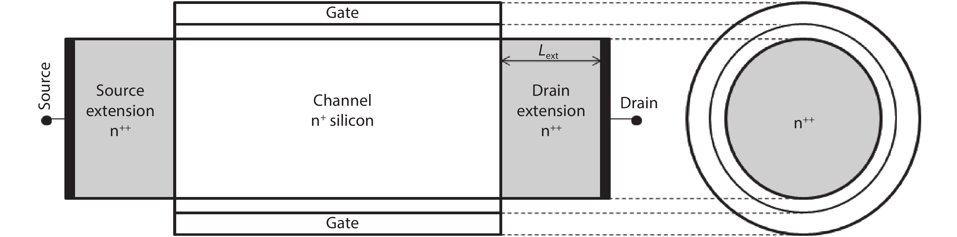
    Fig. 2. GAAJ MOSFET with S/D extensions regions.
    (Color online) n-type JLDG MOSFET structure.
    Fig. 3. (Color online) n-type JLDG MOSFET structure.
    (Color online) Structure of DSBO-SOI MOSFET.
    Fig. 4. (Color online) Structure of DSBO-SOI MOSFET.
    JL DG MOSFET for underlapping at the source end of the channel region.
    Fig. 5. JL DG MOSFET for underlapping at the source end of the channel region.
    JL DG MOSFET for underlapping at the drain end of the channel region.
    Fig. 6. JL DG MOSFET for underlapping at the drain end of the channel region.
    (Color online) Structure of silicon-based MOSFET.
    Fig. 7. (Color online) Structure of silicon-based MOSFET.
    (Color online) Design of BP JL RC MOSFET.
    Fig. 8. (Color online) Design of BP JL RC MOSFET.
    Structure of DMSG MOSFET.
    Fig. 9. Structure of DMSG MOSFET.
    (Color online) Structure of an n-type GC-DMGJLT.
    Fig. 10. (Color online) Structure of an n-type GC-DMGJLT.
    (Color online) Junctionless MOSFET with a cavity for detecting biomolecules.
    Fig. 11. (Color online) Junctionless MOSFET with a cavity for detecting biomolecules.
    Structure of a pocket n-MOSFET.
    Fig. 12. Structure of a pocket n-MOSFET.
    Structure of EJ-SOI MOSFET.
    Fig. 13. Structure of EJ-SOI MOSFET.
    Design of cylindrical surrounding gate MOSFET using dual material.
    Fig. 14. Design of cylindrical surrounding gate MOSFET using dual material.
    Double Gate junctionless MOSFET with extensions and engineering of gate material.
    Fig. 15. Double Gate junctionless MOSFET with extensions and engineering of gate material.
    (Color online) Junctionless MOSFET with asymmetric gate (AG-JL MOSFET).
    Fig. 16. (Color online) Junctionless MOSFET with asymmetric gate (AG-JL MOSFET).
    Structure of recessed channel MOSFET with transparent gate.
    Fig. 17. Structure of recessed channel MOSFET with transparent gate.
    (Color online) Proposed 6-T SRAM cell using junctionless SOI transistor with the connection.
    Fig. 18. (Color online) Proposed 6-T SRAM cell using junctionless SOI transistor with the connection.
    (Color online) Structure of n-type junctionless double gate MOSFET.
    Fig. 19. (Color online) Structure of n-type junctionless double gate MOSFET.
    (Color online) Dual metal gate (DMG) with recessed source and drain UTB SOI MOSFET.
    Fig. 20. (Color online) Dual metal gate (DMG) with recessed source and drain UTB SOI MOSFET.
    ParameterION (A/μm) IOFF (A/μm) ION/IOFFSS (mV/dec)DIBL (mV/V)Channel length (nm)Application
    (GC-DMGJL) MOSFET[22]7.695 × 10–43.741 × 10–102.057 × 10673.422115Analog circuit
    AG-JL MOSFET[28]127 × 10–41 × 10–151.27 × 105686520Digital circuit
    (DMSG) MOSFET[21]1.053 × 10–1664.797810Digital circuit
    JLDG[32]4.86 × 10962.3275.9820Analog/RF
    DGJL MOSFET[27]4.03 × 10963.3479.5820Analog/RF
    Table 1. Comparison of performance parameters of different MOSFET structures.
    Namrata Mendiratta, Suman Lata Tripathi. A review on performance comparison of advanced MOSFET structures below 45 nm technology node[J]. Journal of Semiconductors, 2020, 41(6): 061401
    Download Citation