
Namrata Mendiratta, Suman Lata Tripathi. A review on performance comparison of advanced MOSFET structures below 45 nm technology node[J]. Journal of Semiconductors, 2020, 41(6): 061401
- Journal of Semiconductors
- Vol. 41, Issue 6, 061401 (2020)
Abstract
1. Introduction
A conventional MOSFET maintains its performance beyond 100 nm. Several adverse effects arise due to reduction in channel length reduction depending on scaling trends[
In this paper, a comparison is made among different advance MOSFET structures on the basis of their ON and OFF-state performance. The ON and OFF-state performance are the deciding factor in future scaling trends of new transistor structures. The design of MOSFET structures also depends on different applications such as digital circuit, memory, analog/RF and biomedical applications. The paper describes application based MOSFET designs by exploring DC and AC performance parameters. Several MOSFET designs are implemented to check their circuit performance using circuit simulators available in TCAD tool. Such a prefabrication transistor structure and circuit design analysis plays an important role in achieving the desired performance and also to reduce failure or defect in the fabricated sample.
2. Performance parameter
In general, the MOSFET structures are evaluated on the basis of their subthreshold performance and analog/RF performance. The important MOSFET parameters are needed to be discussed before any comparison among different MOSFET structures.
2.1. Subthreshold performance parameters
The region of operation before MOSFET channel inversion is known as the subthreshold region. The subthreshold parameters are a deciding factor to obtain a desired and reliable MOSFET performance.
2.1.1. Threshold voltage
The minimum amount of gate to source voltage required for channel inversion is known as MOSFET threshold voltage (VT). The value of threshold voltage depends mainly on surface potential which is the voltage of MOSFET capacitor surface (top layer of polysilicon or metal above the oxide) and voltage in the bulk of MOSFET.
2.1.2. OFF-state current
When the voltage of the gate is less than the threshold voltage the MOSFET is considered to be in OFF-state. However, in OFF-state there is a flow of current due to minority charge carriers between the drain and source. This current is known as subthreshold current.
2.1.3. ON-state current
When the voltage of the gate is more than the threshold voltage of the MOSFET. The MOSFET is said to be in ON-state. The flow of current in this state is known as ON current denoted by Ion. The movement of electrons takes place from source to drain.
2.1.4. DIBL (drain induced barrier lowering)
It is a short channel effect in which threshold voltage reduces originally at high drain voltage. When the length of the channel is short drain it is close enough to the gate, at high drain voltage the bottleneck opens and the transistor turns on prematurely. The value of DIBL should be as low as possible to obtain ideal output characteristic of MOS transistors reducing threshold voltage variations due to drain field effect on channel potential.
2.1.5. Subthreshold slope (SS)
In the subthreshold region, the gate terminal controls the drain current and the current is exponentially decreased. The slope of the drain current plot and gate voltage with drain, bulk and source voltages fixed gives subthreshold slope. A suitable value of subthreshold slope (~60 mV/decade) is required to limit the heating effect in short channel devices. The subthreshold slope can be expressed as:
2.2. Analog/RF performance parameters
The analog and RF performance mainly depends on transconductance, transistor capacitances, stability factor and cutoff frequency, etc.
2.2.1. Transconductance
Transconductance is the ratio of drain current variation with respect to the gate voltage of transistor over a small interval of time in the drain current versus gate voltage curve. It is represented as gm[
2.2.2. Junction capacitance
Due to the depletion of charge between the source/drain and substrate the junction capacitances in MOSFET is formed. The charged depletion is changed according to the source/drain voltage. When the voltage of the gate exceeds the threshold voltage there is a formation of the channel at the surface. The junction capacitances are deciding factors for small signal analysis of transistor in RF range of frequencies.
2.2.3. Stability factor
The stability factor (K) mainly depends on two-port equivalent circuit parameters of MOS transistors. It decides the conditional or unconditional stability of transistors in RF range of frequencies. The stability factor can be expressed as[
Here, Y11 and Y22 are input and output admittance parameters at port 1 and 2 respectively. The Y12 and Y21 are called as transfer admittances.
2.2.4. Critical frequency
The critical frequency (fk) is essential for a small signal transistor model and also important to maintain a suitable AC transistor gain and frequency bandwidth. The critical frequency can be calculated at stability factor K= 1. The critical frequency mainly depends on MOSFET capacitance (Cgs, Cgd, and Cds etc.) and other parasitic capacitances. The critical frequency can be expressed as[
Here, fT, gds, Rds and Rgs are the frequency at unity gain, output conductance, drain to source and gate to source resistances respectively. Also, the M and N values are calculated in terms of Cgs and Cgd respectively.
3. Device structure and dimensions
Sarkar et al.[
![]()
Figure 1.TM-DG MOSFET structure.
The material of the gate having the larger work function in place close to the source and the material which is having the lesser work function is placed close to the drain. Polysilicon gates have depletion width of polysilicon and penetration effect of dopant so metal gates are used. The thickness of the Si film is 10 nm and SiO2 is 2 nm. The concentration of dopant of the source and drain is considered to be 1020 cm–3. The ratio of the length of the three material is taken as (L1 : L2 : L3 = 1 : 1 : 0). The doping concentration of the p substrate is taken as 1016 cm–3. Djeffal et al.[
![]()
Figure 2.GAAJ MOSFET with S/D extensions regions.
By including the heavily doped extensions the drain current improves. The GAAJ MOSFET having extensions has high current when compared to conventional GAAJ. The highly doped regions have increased ion current magnitude by 70%. Abhinav et al.[
![]()
Figure 3.(Color online) n-type JLDG MOSFET structure.
The dimensions of device parameters and gate work function is 5.2 eV, the thickness of front gate oxide is 1 nm, the thickness of back gate is 1 nm, the thickness of silicon substrate 5 nm, doping concentration Nd is 3 × 1019 cm–3, length of the channel L is 20 nm. Ouruji et al.[
![]()
Figure 4.(Color online) Structure of DSBO-SOI MOSFET.
Ajay et al.[
![]()
Figure 5.JL DG MOSFET for underlapping at the source end of the channel region.
![]()
Figure 6.JL DG MOSFET for underlapping at the drain end of the channel region.
Kwon et al.[
![]()
Figure 7.(Color online) Structure of silicon-based MOSFET.
The device parameters are the length of gate given as 100 nm, thickness gate oxide is 3 nm, bottom oxide thickness is 10 nm, width of barrier is 10 nm, depth of barrier 75 nm, drain and source doping and substrate are 1 × 10²⁰ and 1 × 1017 cm–3, respectively. Kumar et al.[
![]()
Figure 8.(Color online) Design of BP JL RC MOSFET.
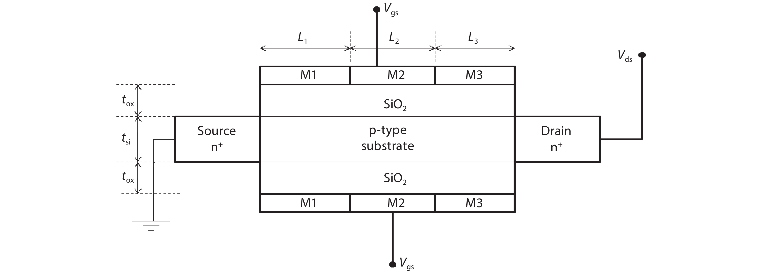
Djeffal et al.[
![]()
Figure 9.Structure of DMSG MOSFET.
The device parameters are Na is 1015 cm–3, drain and source doping is 1020 cm–3, the length L is 10 nm, the thickness of oxide is 2 nm, silicon thickness is 10 nm, L1 and L2 is L/2.
Pathak et al.[
![]()
Figure 10.(Color online) Structure of an n-type GC-DMGJLT.
Ajay et al.[
![]()
Figure 11.(Color online) Junctionless MOSFET with a cavity for detecting biomolecules.
The dimensions of the device are tbio = 9 nm, tox1 = 1 nm, tsi = 10 nm, doping of the source, drain and channel is 1 ×1025 m–3. Length of the cavity is L1 and L3 is 25 nm, and L3 length of the oxide Al2O3 is 50 nm. Pang et al.[
![]()
Figure 12.Structure of a pocket n-MOSFET.
The device parameters are channel length which is 0.1 μm, the thickness of oxide is 4 nm, the junction depth (rj) is 0.06 μm, the doping concentration of the pocket (NP) is 1.906 × 1018 cm–3 and doping concentration in the center region (Nc) is 2.175 × 1017 cm–3, length of the pocket (LP) is 0.024 μm. Orouji et al.[
![]()
Figure 13.Structure of EJ-SOI MOSFET.
The device parameters given are doping of silicon thin layer is 6 × 1016 cm–3, source and drain doping is 5 × 1019 cm–3, the side gates work function is 4.7 eV, the main gate work function is 4.9 eV, thickness of silicon thin layer is 50 nm, thickness of buried oxide is 500 nm, thickness of gate oxide is 2 nm, thickness of barrier diffusion layer is 2 nm, length of main gate is 50 nm and length of total side gate is 50 nm. Pal et al.[
![]()
Figure 14.Design of cylindrical surrounding gate MOSFET using dual material.
The work function of gold (Au ΦM1 4.8 eV), work function of cadmium (Cd) is 4.0 eV. The channel doping of p-type is 6 × 1016 cm–3, n+ source and drain doping region is 5 ×1019 cm–3. Chebaki et al.[
![]()
Figure 15.Double Gate junctionless MOSFET with extensions and engineering of gate material.
The parameters of the devices are doping concentration Nd is 5 × 1018 cm–3, doping of the extension is 5 × 1019 cm–3, thickness of silicon tSi is 10 nm, L is 100 nm, L1 and L2 is L/2, the metal (M1) work function is 5.1 eV, metal (M2) work function is 4.5 eV. Wang et al.[
![]()
Figure 16.(Color online) Junctionless MOSFET with asymmetric gate (AG-JL MOSFET).
The structure parameters are an oxide (HfO2) with EOT 1 nm, channel doping is 1 × 1019 cm–3, length of gate is 20 nm, thickness of silicon is 6 nm. Kumar et al.[
![]()
Figure 17.Structure of recessed channel MOSFET with transparent gate.
The length of the channel (Lg) is 30 nm, width of the device is 200 nm, depth of the groove is 38 nm, junction depth of source and drain is 30 nm, Negative junction depth (NJD) is 10 nm, doping of the substrate (Na) is 1 × 1016 cm–3, doping of source and drain (Nd) is 1 × 1019 cm–3, thickness of physical oxide (tox) is 2 nm. SiO2 permittivity εox is 3.9, gate to source voltage (Vgs) is 0.7 V, drain to source voltage (Vds) 0.5 V, TGRC-MOSFET work function for (ΦITO) is 4.7 eV, CRC-MOSFET work function (ΦM) is 4.2 eV. Mishra et al.[
![]()
Figure 18.(Color online) Proposed 6-T SRAM cell using junctionless SOI transistor with the connection.
The dimensions of the structure is gate length 18 nm, Tox 1 nm, Tsi channel thickness 10 nm, substrate thickness 10 nm, doping density in substrate regions 1 × 1018 cm–3, doping density channel 1 × 1018 cm–3, work function of gate material 4.9 eV.
Roy et al.[
![]()
Figure 19.(Color online) Structure of n-type junctionless double gate MOSFET.
Saramekala et al.[
![]()
Figure 20.(Color online) Dual metal gate (DMG) with recessed source and drain UTB SOI MOSFET.
Work-function of control gate (ΦM1) is 4.8 eV (gold), work-function of screen gate (ΦM2) is 4.6 eV (molybdenum), doping of the channel (Na) is 1015 cm–3, doping of source and drain (Nd) is 1020 cm–3, doping of substrate (Nsub) is 1015 cm–3, oxide thickness of channel (tox) is 1.5–4 nm, thickness of buried (tbox) is 100–300 nm, thickness of recessed is (trsd) 30–100 nm, length of recessed (dbox) is 3 nm, length of the channel (L) is 30–300 nm.
4. Performance comparison and discussion
The performance comparison of different double gate MOSFET has been shown in Table 1 for sub 20 nm technology node including their applications. Since multiple gate MOSFETs have more control of gate over the channel, therefore different DG MOSFET have been considered for performance comparison. Metal gates with high work function are suitable for low OFF-state leakage. The underlap asymmetrical gate increases fringing electric field and leads to better ON-state transistor performance. The absence of depletion region between source/channel and drain in junction-less transistor, improves transistor current drive capability by increasing ON-state current. The high-K dielectric material is preferred as oxide region under gate to improve subthreshold performance parameters and improved switching behavior of transistor. The comparison 20 nm junctionless double gate (JLDG) MOSFET[
5. Conclusion
Various structures of MOSFET have been explored with their structural details and dimensions including applications. Modification in the structure of MOSFET has been done mainly to reduce the short channel effects that include DIBL and SS values. The main motive of these structures is to increase the ON-state current and reduce the OFF-state current. The MOSFET structures are also analyzed for suitable analog/RF performance parameters to obtain a desired range of transconductance, transistor gain, stability factor and critical frequencies. The comparisons between different structures are done on the basis of subthreshold and analog/RF performance parameters. As per comparison made, the junctionless double gate (JLDG) MOSFET provides the lowest subthreshold slope and maximum ION/IOFF ratio for channel length 20 nm. The lowest DIBL obtained from graded channel dual material gate junctionless with channel length 15 nm. Gate engineered transistors of high work function metal contact with various high-K dielectric regions are found suitable to obtain improved subthreshold performance. This shows that gate-engineered multi-gate juntionless MOSFET has good potential to meet future scaling trends with increased compatibility in CMOS technology for any digital/analog and portable IoT or biomedical applications.
References
[1] H H Radamson. CMOS past, present and future. Woodhead Publishing Series in Electronic and Optical Materials(2018).
[2] B Buvaneswari, N B Balamurugan. 2D analytical modeling and simulation of dual material DG MOSFET for biosensing application. Int J Electron Commun, 99, 193(2019).
[3] V M Srivastava, K S Yadav, G Singh. Design and performance analysis of double-gate MOSFET over single-gate MOSFET for RF switch. Microelectron J, 43, 873(2012).
[4] J P Colinge. Multi-gate SOI MOSFETs. Microelectron Eng, 84, 2071(2007).
[5] E Gili, V D Kunz, C H D Groot et al. Single, double and surround gate vertical MOSFETs with reduced parasitic capacitance. Solid-State Electron, 48, 511(2004).
[6] J H K Verma, Y Pratap, S Haldar et al. Capacitance modeling of gate material engineered cylindrical/surrounded gate MOSFETs for sensor applications. Superlattices Microstruct, 88, 271(2015).
[7] I M Tienda-Luna, J B Roldan, F G Ruiz et al. An analytical mobility model for square gate-all-around MOSFETs. Solid-State Electron, 90, 18(2013).
[8] F Djeffal, H Ferhati, T Bentrcia. Improved analog and RF performances of gate-all-around junctionless MOSFET with drain and source extensions. Superlattices Microstruct, 90, 193(2016).
[9] A Sarkar, A K Das, S De et al. Effect of gate engineering in double-gate MOSFETs for analog/RF applications. Microelectron J, 43, 873(2012).
[10] F Nasri, M F B Aissa, M H Gazzah et al. 3D thermal conduction in ananoscale tri-Gate MOSFET based on single-phase-lag model. Appl Therm Eng, 91, 647(2015).
[11] J E Pakaree, V M Srivastava. Realization with fabrication of double-gate MOSFET based differential amplifier. Microelectron J, 91, 70(2019).
[12] S Abhinav. Reliability analysis of junction-less double gate (JLDG) MOSFET for analog/RF circuits for high linearity applications. Microelectron J, 64, 60(2017).
[13] V M Srivastava, K S Yadav, G Singh. Design and performance analysis of cylindrical surrounding double-gate MOSFET for RF switch. Microelectron J, 42, 1124(2011).
[14] W H Ku. Unilateral gain and stability criterion of active two-ports in terms of scattering parameters. Proc IEEE, 54, 1617(1966).
[15] K Sivasankaran, D Kannadassan, K Seetaram et al. Bias and geometry optimization of silicon nanowire transistor: radio frequency stability perspective. Micro Optic Technol Lett, 54, 2114(2012).
[16] A A Orouji, S Heydari, M Fathipour. Double step buried oxide (DSBO) SOI-MOSFET: A proposed structure for improving self-heating effects. Physica E, 41, 1665(2009).
[17] I Kwona, H I Kwonb, H I Cho. Development of high temperatureoperation silicon based MOSFET for harsh environment application. Results Phys, 11, 475(2018).
[18]
[19] R Narang, M Saxena, M Gupta. Modeling of gate underlap junctionless double gate MOSFET as bio-sensor. Mater Sci Semicond Process, 71, 240(2017).
[20] A Kumar, M M Tripathi, R Chaujar. Comprehensive analysis of sub-20 nm black phosphorus based junctionless-recessed channel MOSFET for analog/RF applications. Superlattices Microstruct, 116, 171(2018).
[21] F Djeffal, N Lakhdar, A Yousfi. An optimized design of 10-nm-scale dual-material surrounded gate MOSFETs for digital circuit applications. Physica E, 44, 339(2011).
[22] V Pathak, G Saini. A Graded channel dual-material gate junctionless MOSFET for analog applications. Proced Comput Sci, 125, 825(2018).
[23] R Narang, M Saxena, M Gupta. Investigation of dielectric modulated (DM) double gate (DG) junctionless MOSFETs for application as a biosensors. Superlattices Microstruct, 85, 557(2015).
[24] Y S Pang, J R Brews. Design of 0.1-
[25] A A Orouji, M J Kumar. Nanoscale SOI MOSFETs with electrically induced source/drain extension: Novel attributes and design considerations for suppressed short-channel effects. Superlattices Microstruct, 39, 395(2006).
[26] A Pal, A Sarkar. Analytical study of dual material surrounding gate MOSFET to suppress short-channel effects (SCEs). Eng Sci Technol, 17, 205(2014).
[27] E Chebaki, F Djeffal, H Ferhati et al. Improved analog/RF performance of double gate junctionless MOSFET using both gate material engineering and drain/source extensions. Superlattices Microstruct, 92, 80(2016).
[28] Y Wang, Y Tang, L L Sun et al. High performance of junctionless MOSFET with asymmetric gate. Superlattices Microstruct, 97, 2016(2016).
[29] B Awadhiya, P N Kondekar, A D Meshram. Understanding negative differential resistance and region of operation in undoped HfO2-based negative capacitance field effect transistor. Appl Phys A, 125, 427(2019).
[30] A Kumar, N Gupta, R Chaujar. TCAD RF performance investigation of transparent gate recessed channel MOSFET. Microelectron J, 49, 36(2016).
[31] V K Mishra, R K Chauhan. Efficient layout design of junctionless transistor based 6-T SRAM cell using SOI technology. ECS J Solid State Sci Technol, 9, 456(2018).
[32] N C Roy, A Gupta, S Rai. Analytical surface potential modeling and simulation of junction-less double gate (JLDG) MOSFET for ultra-low power analog/RF circuits. Microelectron J, 46, 916(2015).
[33] G K Saramekala, A Santra, S Dubey et al. An analytical threshold voltage model for a short-channel dual-metal-gate (DMG) recessed-source/drain (Re-S/D) SOI MOSFET. Superlattices Microstruct, 60, 580(2013).
[34] S L Tripathi, R Patel, V K Agrawal. Low leakage pocket junction-less DGTFET with bio sensing cavity region. Turk J Electr Eng Comput Sci, 27, 2466(2019).

Set citation alerts for the article
Please enter your email address
© Copyright 2018-2021 | Chinese Laser Press. All Rights Reserved 沪ICP备15018463号-20