• Journal of Inorganic Materials
  • Vol. 36, Issue 7, 779 (2021)
Hui WANG1、2, Shujuan ZHANG1、3, Tingwei CHEN1, Chuanlin ZHANG1, Haosu LUO2, and Renkui ZHENG1、*
Author Affiliations
  • 11. Jiangxi Engineering Laboratory for Advanced Functional Thin Films, School of Materials Science and Engineering, Nanchang University, Nanchang 330031, China
  • 22. Shanghai Institute of Ceramics, Chinese Academy of Sciences, Shanghai 200050, China
  • 33. School of Materials, Mechanic, and Electrical Engineering, Jiangxi Science and Technology Normal University, Nanchang 330038, China
  • show less
    DOI: 10.15541/jim20200540 Cite this Article
    Hui WANG, Shujuan ZHANG, Tingwei CHEN, Chuanlin ZHANG, Haosu LUO, Renkui ZHENG. Electronic Property of PdSe2 Thin Films Fabricated by Post-selenization of Pd Films[J]. Journal of Inorganic Materials, 2021, 36(7): 779 Copy Citation Text show less
    Side and top view of the crystal structure of PdSe2 thin films (a), schematic illustration for the growth of PdSe2 films on SiO2/Si substrates by post-selenization of a Pd layer in an evacuated quartz ampule (b), and structure diagram of the PdSe2/SiO2/Si structure (c)
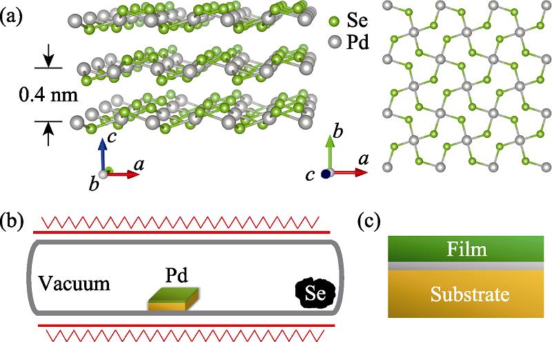
    1. Side and top view of the crystal structure of PdSe2 thin films (a), schematic illustration for the growth of PdSe2 films on SiO2/Si substrates by post-selenization of a Pd layer in an evacuated quartz ampule (b), and structure diagram of the PdSe2/SiO2/Si structure (c)
    Photograph of an as-synthesized 5 mm×5 mm PdSe2 thin film (a), and top-view micrographs of the films selenized at 200 (b), 250 (c), 300 (d), 450 (e), and 600 ℃ (f), respectively
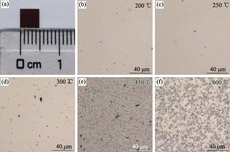
    2. Photograph of an as-synthesized 5 mm×5 mm PdSe2 thin film (a), and top-view micrographs of the films selenized at 200 (b), 250 (c), 300 (d), 450 (e), and 600 ℃ (f), respectively
    Raman spectra (a), FWHM of the Ag3 peaks (b) and Se/Pd atomic ratios (c) of the PdSe2 thin films selenized at different temperatures, cross-sectional HRTEM images for a film selenized at 300 ℃(d-e)
    3. Raman spectra (a), FWHM of the Ag3 peaks (b) and Se/Pd atomic ratios (c) of the PdSe2 thin films selenized at different temperatures, cross-sectional HRTEM images for a film selenized at 300 ℃(d-e)
    Hall resistivity (a), carrier concentration (b), carrier mobility (c), and MR (d) of PdSe2 thin films fabricated at different selenization temperaturesInset in (b) is conductivities of different PdSe2 thin films. Dashed lines in (b, c) represent the carrier density and mobility of the Pd layer
    4. Hall resistivity (a), carrier concentration (b), carrier mobility (c), and MR (d) of PdSe2 thin films fabricated at different selenization temperaturesInset in (b) is conductivities of different PdSe2 thin films. Dashed lines in (b, c) represent the carrier density and mobility of the Pd layer
    MethodMobility/(cm2·V-1·s-1)Ref.
    Exfoliation20.0[13]
    Exfoliation14.0[18]
    Exfoliation0.9[35]
    Exfoliation1.8[36]
    Vacuum selenization48.5This work
    Table 1.

    Comparison of the hole carrier mobility of our p-type PdSe2 with other thin films

    Hui WANG, Shujuan ZHANG, Tingwei CHEN, Chuanlin ZHANG, Haosu LUO, Renkui ZHENG. Electronic Property of PdSe2 Thin Films Fabricated by Post-selenization of Pd Films[J]. Journal of Inorganic Materials, 2021, 36(7): 779
    Download Citation