Abstract
At present, the approaches to fabricate PdSe2 thin films mainly focus on mechanical exfoliation and chemical vapor deposition. In this study, we report a simple and efficient method to fabricate PdSe2 thin films on SiO2/Si substrates. Firstly, a Pd metal layer was deposited on a SiO2/Si substrate using magnetron sputtering. Then the PdSe2 thin film was obtained through selenization of the Pd layer at certain temperatures in a vacuum quartz ampule containing Se powder. According to the cross-sectional high-resolution transmission electron microscopy (HRTEM) image, the as-grown PdSe2 thin film has an average thickness of about 30 nm. The correlation between selenization temperature and electronic transport properties of PdSe2 thin films was investigated. PdSe2 thin films with a hole carrier concentration of ~1018 cm-3 and a mobility of ~48.5 cm2·V-1·s-1 are realized at a low selenization temperature of 300 ℃. It is worth noting that the mobility obtained by the vacuum selenization is superior to that of the p-type PdSe2 thin films fabricated by mechanical exfoliation from bulk PdSe2 single crystals. In addition, a relatively large room-temperature magnetoresistance (MR) of 12% is achieved for the PdSe2 thin films selenized at 300 ℃. With the increase in the selenization temperature from 300 ℃, mobility and magnetoresistance decrease due to the evaporation of Se element at high temperatures. This work demonstrates that present one-step selenization process is a facile and efficient approach to synthesize PdSe2 films, which could actually be used to prepare PdSe2 films in a large scale and may have potential applications for next-generation electronic and magneto-electronic devices.In recent years, the discovery of graphene has aroused substantive interests in two-dimensional (2D) materials for their unique structures and extraordinary electronic properties, opening up a completely new avenue for the development of nanoscale electronics. For electronic and photonic applications, a desirable 2D material have to be air-stable and possess high carrier mobility, high on/off ratio as well as widely tunable bandgap[1]. However, the inherent lack of bandgap limits the practical applications of graphene in electronics. Among several classes of graphene-like layered compounds, transition metal dichalcogenides (TMDCs) (MX2, M = W, S, Mo, etc.; X = S, Se, Te, etc.) are the most studied groups for their tunable energy bandgap and extraordinary properties, which have been regarded as the primary potential alternative candidates for graphene[1,2]. TMDCs, with a typical layered structure in which atoms are connected by strong covalent bondings within each layer whereas bound by weak van der Waals forces between layers, have been proved to possess significantly outstanding properties, such as the thickness-dependent bandgaps[3], extremely large magnetoresistance (MR)[4], superconductivity[5,6], high mobility and high on/off ratio[7,8], manifesting great potential for the future design of transistors[1,8], photodetectors[9,10], and memory devices[11].
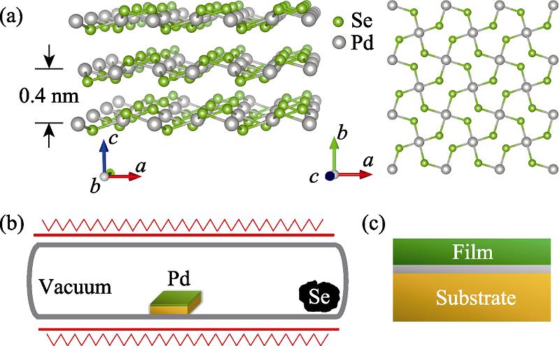
Distinct from the vastly investigated TMDCs including MoS2, WS2 and WSe2, the layers in newly found 2D PdSe2 are interestingly puckered (Fig. 1(a)), which can lead to exotic properties of the in-plane anisotropic in response to external stimuli. Coupled with the buckled structure, the unique planar pentagonal configuration further breaks the sublattice symmetry, which can enhance the spin-orbit coupling and thus allows easily tuning of the electrical properties[12,13]. This kind of puckered pentagonal structures are highly desirable for 2D materials due to the low-symmetry and potential anisotropy properties[14,15] and are expected to result in fascinating new properties and open up possibility for future electronic, optoelectronic, spintronic and valleytronic applications. For example, pentagonal graphene is supposed to realize a large bandgap and ultrahigh mechanical strength[16], and penta-SnS2 has been theoretically predicted to be a 2D Quantum Spin Hall (QSH) insulator with sizable bandgap at room temperature[17]. Although PdSe2 had been demonstrated being stable in air several years ago, it was not until 2017 that the single-layer and few-layer PdSe2 films were successfully synthesized and investigated experimentally in detail[13]. In that experiment, PdSe2 film was reported to display high electron field-effect mobility of 158 cm2·V-1·s-1, a high on/off ratio up to 106 and tunable bandgap from 0 (bulk) to ~1.3 eV (monolayer)[13]. Furthermore, it is revealed that FETs made from PdSe2 films behave ambipolar characteristics and can realize electron field-effect mobility of 216 cm2·V-1·s-1[18]. Later on, the PdSe2 film based photodetector was found to exhibit excellent responsivity (708 mA·W-1) and extremely high external quantum efficiency (EQE) (82700%)[19]. Otherwise, PdSe2 possesses outstanding thermoelectric performance[20], pressure-induced structure transition[21,22] and superconductivity[23]. Most of the PdSe2 materials mentioned above are electron-transport-dominated. However, hole-transport-dominated PdSe2 films are also desired, which are more difficult to obtain, sometimes even a p-type chemical dopant (such as F4-TCNQ[18], TCNQ[24]) is required. Thus, it still remains plenty of room for scientific exploration of PdSe2 thin films.

Figure 1.Side and top view of the crystal structure of PdSe2 thin films (a), schematic illustration for the growth of PdSe2 films on SiO2/Si substrates by post-selenization of a Pd layer in an evacuated quartz ampule (b), and structure diagram of the PdSe2/SiO2/Si structure (c)
To date, the approaches to synthesizing PdSe2 have mainly focused on mechanical exfoliation[13,18] and molecular beam evaporation (MBE)[25], which limits the scalable preparation and extensive application of PdSe2. The post-selenization of metal layers has been proved to be an effective method to prepare MoS2, WS2 and MoSe2 thin films[26,27], and PdSe2 thin films have been successfully fabricated by the chemical vapor transport based on post-selenization of Pd layer[28,29], but detailed investigations are absent. In this work, PdSe2 thin films were successfully fabricated by post-selenization of Pd layers and p-type conducting behavior was confirmed by Hall measurements. The effects of selenization temperature on the electrical and magnetotransport behaviors of the films have been investigated, and the optimum selenization conditions were derived. It was found that PdSe2 films obtained by selenization at 300 ℃ showed the highest carrier mobility of 48.5 cm2·V-1·s-1 and maximum MR of 12% at B=9 T. This study supplements the research of PdSe2 thin films and provides a simple approach for the fabrication of PdSe2 films at a relatively low temperature.
1 Experimental
1.1 Semiconductor film growth
The PdSe2 thin films were synthesized through the post-selenization of Pd layers. At first, Pd seed layers (~20 nm) were deposited on SiO2/Si substrates (5 mm× 5 mm) using a Kurt J. Lesker Magnetron Sputtering System at room temperature. The base pressure of the sputtering chamber was 6.4×10⁻⁶ Pa. The working Ar pressure was kept at 0.4 Pa, and the magnetron source power was set to 20 W. The sputtering time was 60 s. Then, the as-deposited Pd films were immediately sealed in the center of an evacuated quartz ampule, together with 0.01 g Se powder in the bottom, as shown in Fig. 1(b). PdSe2 thin films were obtained by the direct selenization process, which was achieved by simply heating the sealed ampules at different fixed temperatures for 1 h and cooled to room temperature naturally. The schematic structure of the as-prepared thin film is shown in Fig. 1(c).
1.2 Characterization
The Raman spectroscopy and optical microscopy images of the as-selenized thin films were obtained by a Witec alpha300R Raman spectrometer equipped with a 532 nm excitation source. The element composition of the thin films was determined by energy dispersive X-ray spectroscopy (EDS) measurements using a Zeiss Supra 55 scanning electron microscope. Thickness and cross- sectional high-resolution transmission electron microscopy (HRTEM) images of PdSe2 thin films were recorded using a Tecnai G2F20 S-Twin transmission electron microscope. Electronic transport properties of PdSe2 films including resistance, carrier density, carrier type, and MR were measured by a Physical Property Measurement System (PPMS-9, Quantum Design). The Ag electrodes were sputtered using a Sputtering Coater (VTC-16-3HD, HF-Kejing).
2 Results and discussion
2.1 Film characterization
The sputtered Pd layers were post-selenized at a series of temperatures in evacuated quartz ampules, then the as-prepared thin films were characterized by optical microscope installed on a Raman spectroscope. Surface morphologies of the as-prepared films are shown in Fig. 2 from which one may find that the surfaces of the films selenized at 200, 250 and 300 ℃ are relatively cleaner than those selenized at 450 and 600 ℃. The black dots in Fig. 2(e, f) may be caused by the nucleation of gaseous Se during the cooling process.
Figure 2.Photograph of an as-synthesized 5 mm×5 mm PdSe2 thin film (a), and top-view micrographs of the films selenized at 200 (b), 250 (c), 300 (d), 450 (e), and 600 ℃ (f), respectively
The Raman profiles are presented in Fig. 3(a), with no distinct Raman peaks that can be found in the film selenized at 200 ℃, which reveals that 200 ℃ is too low to initiate the selenization process. Films selenized at and above 250 ℃ all display two strong peaks located at 144, 258 cm-1 and two minor peaks centered at 206, 222 cm-1, respectively. According to the previous studies[18,30], Raman peaks centered at 144 cm-1 (Ag1), 206 (Ag2) and 222 cm-1 (B1g) can be ascribed to the movements of Se atoms, while the peaks at 258 cm-1 (Ag3) is assigned to the relative motion between Se and Pd atoms in PdSe2. The asymmetry of Ag1 peak located at 144 cm-1 is caused by the mixture of Ag1, B1g, B2g, and B3g mode, which matches well with the previous reports[18,30]. As reported by Li, et al[31], Raman spectra of monolayer Pd2Se3 display three distinct peaks with Raman shifts centered at 163, 192.4, and 234.6 cm-1, respectively, thus the existence of impure phase of Pd2Se3 can be excluded. The full-width at half-maximum (FWHM) of Ag3 peak is found to be selenization temperature dependent. As the selenization temperature increases, the FWHM gets increasingly narrower, which indicates that the higher selenization temperature is, more beneficial to improve the crystallinity of the film[32].
Figure 3.Raman spectra (a), FWHM of the Ag3 peaks (b) and Se/Pd atomic ratios (c) of the PdSe2 thin films selenized at different temperatures, cross-sectional HRTEM images for a film selenized at 300 ℃(d-e)
Compositional analysis of the films has been conducted by EDS. As shown in Fig. 3(c), for the films selenized at and below 450 ℃, the Se/Pd atomic ratio is about 2.5. At 600 ℃, there is a re-evaporation of Se, leading to the lack of Se element[33]. Film thickness and crystal structure of the PdSe2 thin films have been measured using cross-sectional HRTEM measurements. As presented in Fig. 3(d), the thickness of the PdSe2 film selenized at 300 ℃ is about 30 nm. According to the literature[28], the thickness of PdSe2 films mostly depends on the thickness of the Pd seed layers, thus one can assume that the thickness of all the films is almost consistent since the initial Pd seed layers obtained is almost consistent. In Fig. 3(e), the cross-sectional HRTEM image with high magnification shows zigzag chains with the lattice spacing of ~0.4 nm on the SiO2/Si substrate, which can be assigned to the (002) plane of PdSe2 as previously reported[18,28,30], further confirming the successful preparation of PdSe2 film.
2.2 Effects of selenization temperature on electrical transport property
The electrical properties of PdSe2 thin films including the Hall resistance (ρxy), carrier density (n), carrier mobility (μ) were studied by the Hall measurements at room temperature. The results are shown in Fig. 4(a-c). The carrier density and mobility of the Pd layer has also been investigated as a blank reference, as presented by the red dashed lines in Fig. 4(b-c). The slopes of the Hall resistance versus magnetic field curves show distinct changes with temperature increasing, which is a signature of the change in carrier density of the PdSe2 films. Note that the slopes are positive for the films selenized at 300, 450 and 600 ℃, indicating that the holes are the majority charge carriers. The carrier density n was obtained by the Hall measurements and the carrier mobility was calculated using the equation s=nμe, where s and e are the conductivity and electron charge, respectively. The carrier density and mobility of the film selenized at 200 ℃ are close to that of Pd metal layer, which is consistent with the Raman result. One may find that the carrier density decreases rapidly from 1×10²² to 1×1018 cm-3 as the selenization temperature increases from 200 to 300 ℃ (Fig. 4 (b)), because most of the Pd layers still remain un-selenized at 200 ℃ or incompletely selenized at 250 ℃ and completely selenized at 300 ℃. The same trend for the conductivity can be obtained through calculation using the aforementioned equation (inset in Fig. 4(b)). However, the carrier density undergoes a slight increase at 600 ℃ because of the re-evaporation of Se at high temperature[33,34]. The variation of mobility with selenization temperature (Fig. 4(c)) shows an opposite trend of carrier concentration and conductivity (Fig. 4(b)). The film selenized at 300 ℃ shows the highest hole mobility of 48.5 cm2·V-1·s-1 and the mobility decreases with further increase of the selenization temperature. The mobility of PdSe2 thin films obtained by vacuum selenization process here is much higher than that of the PdSe2 films fabricated by traditional mechanical exfoliation method[13,18,35-36], as listed in Table 1.
Figure 4.Hall resistivity (a), carrier concentration (b), carrier mobility (c), and MR (d) of PdSe2 thin films fabricated at different selenization temperaturesInset in (b) is conductivities of different PdSe2 thin films. Dashed lines in (b, c) represent the carrier density and mobility of the Pd layer
| Method | Mobility/(cm2·V-1·s-1) | Ref. |
|---|
| Exfoliation | 20.0 | [13] |
| Exfoliation | 14.0 | [18] |
| Exfoliation | 0.9 | [35] |
| Exfoliation | 1.8 | [36] |
| Vacuum selenization | 48.5 | This work |
Table 1.
Comparison of the hole carrier mobility of our p-type PdSe2 with other thin films
2.3 Effects of selenization temperature on magnetoresistance
Magnetoresistance (MR) effect is quite important for magnetoelectronics applications. It is defined as MR(%)=[R(T)-R(0)]/R(0), where R(0) refers to the resistance at B = 0 T. Fig. 4(d) depicts the MR with field sweeping for all the PdSe2 films selenized at various temperatures from 200 to 600 ℃. MR of films selenized at higher temperatures (300, 450 and 600 ℃) are non-saturated, which has also been observed in its analogue WTe2 thin films[4]. As shown in Fig. 4(d), the largest MR is approximately 12% without saturation for the film selenized at 300 ℃ when the field increases to 9 T. These films present a parabolic positive MR, which probably arises from the curved orbits in a magnetic field caused by classical Lorentz force in non-magnetic materials[37]. The variation trend of MR with temperature is consistent with the evolution trend of film’s carrier concentration and mobility as selenization temperature increases from 200 to 600 ℃.
3 Conclusion
In summary, PdSe2 thin films were prepared by post-selenization treatment of magnetron-sputtered Pd layers on SiO2/Si substrates. Investigation on the effects of selenization temperature reveals that films selenized at 300 ℃ show p-type conduction, modest carrier concentration of 1×1018 cm-3, the highest mobility of 48.5 cm2·V-1·s-1 and maximum room-temperature MR of 12% at B=9 T. Selenization temperatures below 250 ℃ and above 600 ℃ produce a degenerative effects on the electrical and magnetotransport property of the films, which are attribute to the incomplete selenization of the Pd layer and easily evaporation of Se at high temperature, respectively. Our work demonstrates that post-selenization of magnetron- sputtered Pd layers is an effective and flexible method to prepare PdSe2 thin films.
References
[1] D JARIWALA, K SANGWAN V, J LAUHON L et al. Emerging device applications for semiconducting two-dimensional transition metal dichalcogenides. ACS Nano, 8, 1102-1120(2014).
[2] Z BUTLER S, M HOLLEN S, L CAO et al. Progress, challenges, and opportunities in two-dimensional materials beyond graphene. ACS Nano, 7, 2898-2926(2013).
[3] H WANG Q, K KALANTAR-ZADEH, A KIS et al. Electronics and optoelectronics of two-dimensional transition metal dichalcogenides. Nature Nanotechnology, 7, 699-712(2012).
[4] N ALI M, J XIONG, S FLYNN et al. Large, non-saturating magnetoresistance in WTe2. Nature, 514, 205-208(2014).
[5] W SHI, J YE, Y ZHANG et al. Superconductivity series in transition metal dichalcogenides by ionic gating. Scientific Reports, 5, 12534(2015).
[6] C NETO A H. Charge density wave, superconductivity, and anomalous metallic behavior in 2D transition metal dichalcogenides. Physical Review Letters, 86, 4382-4385(2001).
[7] V PODZOROV, E GERSHENSON M, C KLOC et al. High- mobility field-effect transistors based on transition metal dichalcogenides. Applied Physics Letters, 84, 3301(2004).
[8] B RADISAVLJEVIC, A KIS. Mobility engineering and a metal-insulator transition in monolayer MoS2. Nature Materials, 12, 815-823(2013).
[9] S TONGAY, J ZHOU, C ATACA et al. Broad-range modulation of light emission in two-dimensional semiconductors by molecular physisorption gating. Nano Letters, 13, 2831-2836(2013).
[10] S TAN, S YIN, G OUYANG. Size effect on the interface modulation of interlayer and auger recombination rates in MoS2/WSe2 van der Waals heterostructures. Journal of Inorganic Materials, 35, 682-688(2020).
[11] C KO, Y LEE, Y CHEN et al. Ferroelectrically gated atomically thin transition-metal dichalcogenides as nonvolatile memory. Advanced Materials, 28, 2923-2930(2016).
[12] C SOULARD, X ROCQUEFELTE, E PETIT et al. Experimental and theoretical investigation on the relative stability of the PdSe2- and pyrite-type structures of PdSe2. Inorganic Chemistry, 43, 1943-1949(2004).
[13] D OYEDELE A, S YANG, B LIANG L et al. PdSe2: pentagonal two-dimensional layers with high air stability for electronics. Journal of the American Chemical Society, 139, 14090-14097(2017).
[14] F XIA, H WANG, Y JIA. Rediscovering black phosphorus as an anisotropic layered material for optoelectronics and electronics. Nature Communications, 5, 4458(2014).
[15] L PHANEUF-L'HEUREUX A, A FAVRON, F GERMAIN J et al. Polarization-resolved Raman study of bulk-like and Davydov- induced vibrational modes of exfoliated black phosphorus. Nano Letters, 16, 7761-7767(2016).
[16] S ZHANG, J ZHOU, Q WANG et al. Penta-graphene: a new carbon allotrope. Proceedings of the National Academy of Sciences of the United States of America, 112, 2372-2377(2015).
[17] Y MA, L KOU, X LI et al. Room temperature quantum spin Hall states in two-dimensional crystals composed of pentagonal rings and their quantum wells. NPG Asia Materials, 8, e264(2016).
[18] L CHOW W, P YU, A LIU F et al. High mobility 2D palladium diselenide field-effect transistors with tunable ambipolar characteristics. Advanced Materials, 29, 1602969(2017).
[19] J LIANG Q, X WANG Q, Q ZHANG et al. High-performance, room temperature, ultra-broadband photodetectors based on air-stable PdSe2. Advanced Materials, 31, 1807609(2019).
[20] F SUN J, L SHI H, T SIEGRIST et al. Electronic, transport, and optical properties of bulk and mono-layer PdSe2. Applied Physics Letters, 107, 153902(2015).
[21] S AHMAD. Strain dependent tuning electronic properties of noble metal dichalcogenides PdX2 (X=S, Se) mono-layer. Materials Chemistry and Physics, 198, 162-166(2017).
[22] W LEI, S ZHANG, G HEYMANN et al. A new 2D high-pressure phase of PdSe2 with high-mobility transport anisotropy for photovoltaic applications. Journal of Materials Chemistry C, 7, 2096-105(2019).
[23] A ELGHAZALI M, G NAUMOV P, H MIRHOSSEINI et al. Pressure-induced superconductivity up to 13.1 K in the pyrite phase of palladium diselenide PdSe2. Physical Review B, 96, 060509(2017).
[24] Z GAO Y, F LIU X, W HU et al. Tunable n-type and p-type doping of two-dimensional layered PdSe2via organic molecular adsorption. Physical Chemistry Chemical Physics, 22, 12973-12979(2020).
[25] E LI, F WANG D, P FAN et al. Construction of bilayer PdSe2 on epitaxial graphene. Nano Research, 11, 5858-5865(2018).
[26] Y JUNG, J SHEN, H LIU Y et al. Metal seed layer thickness- induced transition from vertical to horizontal growth of MoS2 and WS2. Nano Letters, 14, 6842-6849(2014).
[27] S KONG D, T WANG H, J CHA J et al. Synthesis of MoS2 and MoSe2 films with vertically aligned layers. Nano Letters, 13, 1341-1347(2013).
[28] H ZENG L, D WU, H LIN S et al. Controlled synthesis of 2D palladium diselenide for sensitive photodetector applications. Advanced Functional Materials, 29, 1806878(2019).
[29] B LUO L, D WANG, C XIE et al. PdSe2 multilayer on germanium nanocones array with light trapping effect for sensitive infrared photodetector and image sensing application. Advanced Functional Materials, 29, 1900849(2019).
[30] H ZENG L, M CHEN Q, X ZHANG Z et al. Multilayered PdSe2/perovskite Schottky junction for fast, self-powered, polarization-sensitive, broadband photodetectors, and image sensor application. Advanced Science, 6, 1901134(2019).
[31] Y LI X, H ZHANG S, G GUO Y et al. Physical properties and photovoltaic application of semiconducting Pd2Se3 monolayer. Nanomaterials, 8, 832(2018).
[32] A PURETZKY A, D OYEDELE A, K XIAO et al. Anomalous interlayer vibrations in strongly coupled layered PdSe2. 2D Materials., 5, 035016(2018).
[33] T LAKSHMIKUMAR S, C RASTOGI A. Selenization of Cu and in thin films for the preparation of selenide photo-absorber layers in solar cells using Se vapour source. Solar Energy Materials and Solar Cells, 32, 7-19(1994).
[34] H LE P, N LIAO C, W LUO C et al. Thermoelectric properties of bismuth-selenide films with controlled morphology and texture grown using pulsed laser deposition. Applied Surface Science, 285, 657-663(2013).
[35] D BARTOLOMEO A, A PELELLA, W LIU X et al. Pressure- tunable ambipolar conduction and hysteresis in thin palladium diselenide field effect transistors. Advanced Functional Materials, 29, 1902483(2019).
[36] H ZHONG J, J YU, K CAO L et al. High-performance polarization-sensitive photodetector based on a few-layered PdSe2 nanosheet. Nano Research, 13, 1780-1786(2020).
[37] W ZHANG Y, L NING H, N LI Y et al. Negative to positive crossover of the magnetoresistance in layered WS2. Applied Physics Letters, 108, 153114(2016).