• Journal of Inorganic Materials
  • Vol. 36, Issue 7, 779 (2021)
Hui WANG1、2, Shujuan ZHANG1、3, Tingwei CHEN1, Chuanlin ZHANG1, Haosu LUO2, and Renkui ZHENG1、*
Author Affiliations
  • 11. Jiangxi Engineering Laboratory for Advanced Functional Thin Films, School of Materials Science and Engineering, Nanchang University, Nanchang 330031, China
  • 22. Shanghai Institute of Ceramics, Chinese Academy of Sciences, Shanghai 200050, China
  • 33. School of Materials, Mechanic, and Electrical Engineering, Jiangxi Science and Technology Normal University, Nanchang 330038, China
  • show less
    DOI: 10.15541/jim20200540 Cite this Article
    Hui WANG, Shujuan ZHANG, Tingwei CHEN, Chuanlin ZHANG, Haosu LUO, Renkui ZHENG. Electronic Property of PdSe2 Thin Films Fabricated by Post-selenization of Pd Films[J]. Journal of Inorganic Materials, 2021, 36(7): 779 Copy Citation Text show less
    References

    [1] D JARIWALA, K SANGWAN V, J LAUHON L et al. Emerging device applications for semiconducting two-dimensional transition metal dichalcogenides. ACS Nano, 8, 1102-1120(2014).

    [2] Z BUTLER S, M HOLLEN S, L CAO et al. Progress, challenges, and opportunities in two-dimensional materials beyond graphene. ACS Nano, 7, 2898-2926(2013).

    [3] H WANG Q, K KALANTAR-ZADEH, A KIS et al. Electronics and optoelectronics of two-dimensional transition metal dichalcogenides. Nature Nanotechnology, 7, 699-712(2012).

    [4] N ALI M, J XIONG, S FLYNN et al. Large, non-saturating magnetoresistance in WTe2. Nature, 514, 205-208(2014).

    [5] W SHI, J YE, Y ZHANG et al. Superconductivity series in transition metal dichalcogenides by ionic gating. Scientific Reports, 5, 12534(2015).

    [6] C NETO A H. Charge density wave, superconductivity, and anomalous metallic behavior in 2D transition metal dichalcogenides. Physical Review Letters, 86, 4382-4385(2001).

    [7] V PODZOROV, E GERSHENSON M, C KLOC et al. High- mobility field-effect transistors based on transition metal dichalcogenides. Applied Physics Letters, 84, 3301(2004).

    [8] B RADISAVLJEVIC, A KIS. Mobility engineering and a metal-insulator transition in monolayer MoS2. Nature Materials, 12, 815-823(2013).

    [9] S TONGAY, J ZHOU, C ATACA et al. Broad-range modulation of light emission in two-dimensional semiconductors by molecular physisorption gating. Nano Letters, 13, 2831-2836(2013).

    [10] S TAN, S YIN, G OUYANG. Size effect on the interface modulation of interlayer and auger recombination rates in MoS2/WSe2 van der Waals heterostructures. Journal of Inorganic Materials, 35, 682-688(2020).

    [11] C KO, Y LEE, Y CHEN et al. Ferroelectrically gated atomically thin transition-metal dichalcogenides as nonvolatile memory. Advanced Materials, 28, 2923-2930(2016).

    [12] C SOULARD, X ROCQUEFELTE, E PETIT et al. Experimental and theoretical investigation on the relative stability of the PdSe2- and pyrite-type structures of PdSe2. Inorganic Chemistry, 43, 1943-1949(2004).

    [13] D OYEDELE A, S YANG, B LIANG L et al. PdSe2: pentagonal two-dimensional layers with high air stability for electronics. Journal of the American Chemical Society, 139, 14090-14097(2017).

    [14] F XIA, H WANG, Y JIA. Rediscovering black phosphorus as an anisotropic layered material for optoelectronics and electronics. Nature Communications, 5, 4458(2014).

    [15] L PHANEUF-L'HEUREUX A, A FAVRON, F GERMAIN J et al. Polarization-resolved Raman study of bulk-like and Davydov- induced vibrational modes of exfoliated black phosphorus. Nano Letters, 16, 7761-7767(2016).

    [16] S ZHANG, J ZHOU, Q WANG et al. Penta-graphene: a new carbon allotrope. Proceedings of the National Academy of Sciences of the United States of America, 112, 2372-2377(2015).

    [17] Y MA, L KOU, X LI et al. Room temperature quantum spin Hall states in two-dimensional crystals composed of pentagonal rings and their quantum wells. NPG Asia Materials, 8, e264(2016).

    [18] L CHOW W, P YU, A LIU F et al. High mobility 2D palladium diselenide field-effect transistors with tunable ambipolar characteristics. Advanced Materials, 29, 1602969(2017).

    [19] J LIANG Q, X WANG Q, Q ZHANG et al. High-performance, room temperature, ultra-broadband photodetectors based on air-stable PdSe2. Advanced Materials, 31, 1807609(2019).

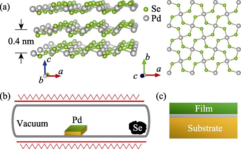
    [20] F SUN J, L SHI H, T SIEGRIST et al. Electronic, transport, and optical properties of bulk and mono-layer PdSe2. Applied Physics Letters, 107, 153902(2015).

    [21] S AHMAD. Strain dependent tuning electronic properties of noble metal dichalcogenides PdX2 (X=S, Se) mono-layer. Materials Chemistry and Physics, 198, 162-166(2017).

    [22] W LEI, S ZHANG, G HEYMANN et al. A new 2D high-pressure phase of PdSe2 with high-mobility transport anisotropy for photovoltaic applications. Journal of Materials Chemistry C, 7, 2096-105(2019).

    [23] A ELGHAZALI M, G NAUMOV P, H MIRHOSSEINI et al. Pressure-induced superconductivity up to 13.1 K in the pyrite phase of palladium diselenide PdSe2. Physical Review B, 96, 060509(2017).

    [24] Z GAO Y, F LIU X, W HU et al. Tunable n-type and p-type doping of two-dimensional layered PdSe2via organic molecular adsorption. Physical Chemistry Chemical Physics, 22, 12973-12979(2020).

    [25] E LI, F WANG D, P FAN et al. Construction of bilayer PdSe2 on epitaxial graphene. Nano Research, 11, 5858-5865(2018).

    [26] Y JUNG, J SHEN, H LIU Y et al. Metal seed layer thickness- induced transition from vertical to horizontal growth of MoS2 and WS2. Nano Letters, 14, 6842-6849(2014).

    [27] S KONG D, T WANG H, J CHA J et al. Synthesis of MoS2 and MoSe2 films with vertically aligned layers. Nano Letters, 13, 1341-1347(2013).

    [28] H ZENG L, D WU, H LIN S et al. Controlled synthesis of 2D palladium diselenide for sensitive photodetector applications. Advanced Functional Materials, 29, 1806878(2019).

    [29] B LUO L, D WANG, C XIE et al. PdSe2 multilayer on germanium nanocones array with light trapping effect for sensitive infrared photodetector and image sensing application. Advanced Functional Materials, 29, 1900849(2019).

    [30] H ZENG L, M CHEN Q, X ZHANG Z et al. Multilayered PdSe2/perovskite Schottky junction for fast, self-powered, polarization-sensitive, broadband photodetectors, and image sensor application. Advanced Science, 6, 1901134(2019).

    [31] Y LI X, H ZHANG S, G GUO Y et al. Physical properties and photovoltaic application of semiconducting Pd2Se3 monolayer. Nanomaterials, 8, 832(2018).

    [32] A PURETZKY A, D OYEDELE A, K XIAO et al. Anomalous interlayer vibrations in strongly coupled layered PdSe2. 2D Materials., 5, 035016(2018).

    [33] T LAKSHMIKUMAR S, C RASTOGI A. Selenization of Cu and in thin films for the preparation of selenide photo-absorber layers in solar cells using Se vapour source. Solar Energy Materials and Solar Cells, 32, 7-19(1994).

    [34] H LE P, N LIAO C, W LUO C et al. Thermoelectric properties of bismuth-selenide films with controlled morphology and texture grown using pulsed laser deposition. Applied Surface Science, 285, 657-663(2013).

    [35] D BARTOLOMEO A, A PELELLA, W LIU X et al. Pressure- tunable ambipolar conduction and hysteresis in thin palladium diselenide field effect transistors. Advanced Functional Materials, 29, 1902483(2019).

    [36] H ZHONG J, J YU, K CAO L et al. High-performance polarization-sensitive photodetector based on a few-layered PdSe2 nanosheet. Nano Research, 13, 1780-1786(2020).

    [37] W ZHANG Y, L NING H, N LI Y et al. Negative to positive crossover of the magnetoresistance in layered WS2. Applied Physics Letters, 108, 153114(2016).

    Hui WANG, Shujuan ZHANG, Tingwei CHEN, Chuanlin ZHANG, Haosu LUO, Renkui ZHENG. Electronic Property of PdSe2 Thin Films Fabricated by Post-selenization of Pd Films[J]. Journal of Inorganic Materials, 2021, 36(7): 779
    Download Citation