Author Affiliations
1Joint International Research Laboratory of Information Display and Visualization, School of Electronic Science and Engineering, Southeast University, Nanjing 210096, China2Science and Technology on Monolithic Integrated Circuits and Modules Laboratory, Nanjing Electronic Devices Institute, Nanjing 210016, China3Key Laboratory of Micro-Inertial Instrument and Advanced Navigation Technology, Ministry of Education, School of Instrument Science and Engineering, Southeast University, Nanjing 210096, Chinashow less
Abstract
This letter presents the fabrication of InP double heterojunction bipolar transistors (DHBTs) on a 3-inch flexible substrate with various thickness values of the benzocyclobutene (BCB) adhesive bonding layer, the corresponding thermal resistance of the InP DHBT on flexible substrate is also measured and calculated. InP DHBT on a flexible substrate with 100 nm BCB obtains cut-off frequency fT = 358 GHz and maximum oscillation frequencyfMAX = 530 GHz. Moreover, the frequency performance of the InP DHBT on flexible substrates at different bending radii are compared. It is shown that the bending strain has little effect on the frequency characteristics (less than 8.5%), and these bending tests prove that InP DHBT has feasible flexibility.This letter presents the fabrication of InP double heterojunction bipolar transistors (DHBTs) on a 3-inch flexible substrate with various thickness values of the benzocyclobutene (BCB) adhesive bonding layer, the corresponding thermal resistance of the InP DHBT on flexible substrate is also measured and calculated. InP DHBT on a flexible substrate with 100 nm BCB obtains cut-off frequency fT = 358 GHz and maximum oscillation frequencyfMAX = 530 GHz. Moreover, the frequency performance of the InP DHBT on flexible substrates at different bending radii are compared. It is shown that the bending strain has little effect on the frequency characteristics (less than 8.5%), and these bending tests prove that InP DHBT has feasible flexibility.Introduction
Flexible electronics have unique advantages of flexibility, ductility and portability, which have wide application prospects in communication information, energy, medical and other fields[1-6]. However, the future application of high frequency communication and wireless internet of things puts forward higher requirements on the frequency of flexible electrons. The current traditional flexible electronic devices and circuits cannot meet the requirements of larger bandwidth and higher speed, because these flexible electronic devices have low carrier mobility and saturation speed in a higher frequency range[7-9]. As a result, high performance RF transistors and circuits with higher speeds and frequencies are in great demand.
At present, various types of flexible electronic materials and devices have been developed and applied, such as graphene/carbon transistor, GaAs HBT/HEMT, Si MOSFET, etc., all of which have their own unique advantages and application fields[10-17]. We have reported a fabrication method for transferring InP DHBTs onto a flexible substrate using benzocyclobutene (BCB) bonding technology lately. The flexible substrate InP DHBT device has the cut off frequencyfT = 337 GHz and oscillation frequencyfMAX = 485 GHz[18]. In this paper, we continue to present an optimized process of the BCB adhesive layer between InP DHBT and the flexible substrate, which can operate at higher cut off frequencyfT = 358 GHz and oscillation frequencyfMAX = 530 GHz, the thermal resistance (Rth) of InP DHBT on flexible substrate is estimated. In addition, the RF performance under different bending radii is also compared.
Fabrication process
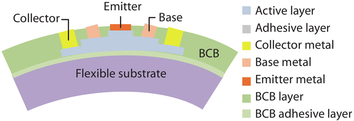
The process of fabricating InP DHBT devices on flexible substrate has been reported in previous work with identical device geometry[18], while the standard 0.5μm process is used for InP DHBT devices.Fig. 1 shows a schematic diagram of InP DHBT devices on flexible substrate.

Figure 1.(Color online) The schematic diagram of InP DHBT device on flexible substrate.
The BCB adhesive layer is sandwiched between InP DHBTs layers and flexible substrate, the thermal conductivity of BCB is 0.3, and InP is 68 W/(m·K), the flexible substrate material used in this letter is boron nitride (BN) composite polymer material, which has a thermal conductivity greater than 8 W/(m·K). Considering the BCB having low thermal conductivity, it is necessary to evaluate the different thickness of BCB adhesive layer which affect the RF andI–V performances of InP DHBT.
The BCB adhesive layer is spun onto two groups of 3-inch flexible substrates with BCB thickness of 100 nm and 1μm, respectively. After the InP DHBT device is bonded to the flexible substrate, the BCB thickness under the InP DHBT device is measured by the focused ion beam (FIB), as shown inFigs. 2(a) and2(b), which shows the FIB image of InP DHBT on the flexible substrate, the thickness of BCB can be measured separately.
Figure 2.(a) FIB cross-sectional image of InP DHBT device on flexible substrate with 1μm BCB. (b) FIB cross-sectional image of InP DHBT device on flexible substrate with 100 nm BCB.
Results and discussions
To make a heat dissipation evaluation of InP DHBT device on flexible substrate, thermal resistance (Rth) of InP DHBT was measured. A large output current leads to an increasing amount of self-heating.Fig. 3 shows the calculated and experimentalRth of fabricated InP DHBT with the emitter area ofAE = 0.5 × 5μm2. The current gain and emitter-base voltage vary with temperature to evaluate thermal resistance of the device,Rth is expressed by the following relation[19]:
Figure 3.(Color online) Experimental and calculatedRth for InP DHBT and flexible substrate InP DHBT.
Table Infomation Is Not Enable
Theϕ is a thermo-electrical coefficient expressed from Gummel plots with different testing temperatures,Vbe is the base-emitter voltage for a constant collector current, theϕ can be expressed as ΔVbe =ϕ · ΔT, the ΔT in junction temperature versus the backplate temperature for a certain powerPdiss dissipated in the InP DHBT. And thePdiss dissipated power variation withPdiss = ΔVce ·Ic. The measuredϕ is about 0.84 mV/K of InP DHBT device. The measuredRth of a conventional InP DHBT device on the InP substrate is 3505 K/W, while the InP DHBT device on a flexible substrate with 100 nm BCB exhibitsRth of 6410 K/W, which is about an 82.8% increase. And the InP DHBT device on a flexible substrate with 1μm BCB exhibitsRth of 7550 K/W, which is attributed to the low thermal conductivity of flexible substrate and BCB.
I–V measurements of flexible substrate InP DHBT devices were performed on a semiconductor wafer probe,Fig. 4 shows the common emitterIC–VCE characteristics of flexible substrate InP DHBT devices with two different thickness of BCB. It can be confirmed that theIC–VCE characteristics of InP DHBT devices with different BCB thicknesses are degraded to a certain extent, and the BCB with the thickness of 1μm is degraded more seriously, this result corresponds to an increase in thermal resistance.
Figure 4.(Color online) The correspondingIC–VCE of InP DHBT and flexible substrate InP DHBT.
The RF performance of flexible substrate InP DHBTs are measured by vector network analyzer, which using off-wafer line-line-reflect-match calibration, at the same time, the device pads are de-embedded with open/short calibration structures[20–23].Fig. 5 shows the InP DHBT short-circuit current gain |h21|2 and Mason’s unilateral gainU on frequency function, when theVCE = 1.5 V and collector currentIC = 15 mA. Using extrapolation ofU and |h21|2 with a –20 dB/dec roll-off yields method, which shows the cut off frequencyfT = 395 GHz, the maximum oscillation frequencyfMAX = 630 GHz of the InP DHBT on InP substrate. For the flexible substrate InP DHBT with 100 nm BCB, the cut off frequencyfT and maximum oscillationfMAX are 358 and 530 GHz respectively.
Figure 5.(Color online) Mason’s unilateral gainU and |h21|2 as a function of frequency measured the InP DHBT and flexible substrate InP DHBT.
The RF performancefT andfMAX of the flexible substrate InP DHBT device in this paper are compared with the performance of other flexible transistors reported previously in Refs. [13,15,17,18,24–27], as shown inTable 1. Our work shows the highest RF frequency performance of flexible devices to date, besides confirms the potential of flexible substrate InP DHBT for high frequency applications.
At the same time, in order to explore the influence of flexible substrate bending on the high-frequency performance of InP DHBT devices, the 3-inch flexible substrate InP DHBT is pasted on curved glass with a certain bending radius[28-30]. The bending degree of flexible substrate depends on the bending radius of curved glass, as shown inFig. 6(a). Three different bending radii of 70, 30 and 15 mm are set to measure the high frequency performance of the flexible substrate InP DHBT.Figs. 6(b) and6(c) show a comparison of the frequency characteristics of InP DHBT at these three bending radii. It is observed that a decrease in the bending radii leads to a slight degradation of the device's high-frequency performance, although in a case there is a small increase infT as the bending increases. ThefT andfMAX of the device in the bent state are reduced by about 8.5% compared with that in the flat state. The performance of InP DHBT devices decreases slightly under different bending states, which may be related to strain, it affects the carrier mobility and other properties of InP DHBT.
Figure 6.(Color online) (a) Photographs of InP DHBT on flexible substrate under bending conditions on test bench. The InP DHBT frequency performance under different bending radii: (b)fT/fT(flat), (c)fMAX/fMAX(flat).
Conclusion
A standard 0.5μm process of InP DHBT is fabricated on 3-inch flexible substrate using epitaxial lift-off and BCB adhesive bonding techniques. Different thickness values of BCB adhesive bonding layer and the corresponding thermal resistance are investigated, besides high cut-off frequencyfT = 358 GHz and maximum oscillationfMAX = 530 GHz are obtained. Moreover, the RF performance under different bending radii is also compared, and the results show that the RF performance of the flexible InP DHBT is less affected by bending strain. These results further confirm the possibility that flexible InP DHBT will be used in flexible RF circuits.
Acknowledgments
This work was supported in part by National Natural Science Foundation of China under Grants 61875241.
References
[1] K H Cherenack, A Z Kattamis, B Hekmatshoar et al. Amorphous-silicon thin-film transistors fabricated at 300 °C on a free-standing foil substrate of clear plastic. IEEE Electron Device Lett, 28, 1004(2007).
[2] S Saxena, D C Kim, J H Park et al. Polycrystalline silicon thin-film transistor using Xe flash-lamp annealing. IEEE Electron Device Lett, 31, 1242(2010).
[3] B Crone, A Dodabalapur, Y Y Lin et al. Large-scale complementary integrated circuits based on organic transistors. Nature, 403, 521(2000).
[4] U Haas, H Gold, A Haase et al. Submicron pentacene-based organic thin film transistors on flexible substrates. Appl Phys Lett, 91, 043511(2007).
[5] T Takahashi, K Takei, E Adabi et al. Parallel array InAs nanowire transistors for mechanically bendable, ultrahigh frequency electronics. ACS Nano, 4, 5855(2010).
[6] E Menard, R G Nuzzo, J A Rogers. Bendable single crystal silicon thin film transistors formed by printing on plastic substrates. Appl Phys Lett, 86, 093507(2005).
[7] J H Ahn, H S Kim, K J Lee et al. High-speed mechanically flexible single-crystal silicon thin-film transistors on plastic substrates. IEEE Electron Device Lett, 27, 460(2006).
[8] Y M Lin, C Dimitrakopoulos, K A Jenkins et al. 100-GHz transistors from wafer-scale epitaxial graphene. Science, 327, 662(2010).
[9] Y Cao, G J Brady, H Gui et al. Radio frequency transistors using aligned semiconducting carbon nanotubes with current-gain cutoff frequency and maximum oscillation frequency simultaneously greater than 70 GHz. ACS Nano, 10, 6782(2016).
[10] Y G Sun, E Menard, J A Rogers et al. Gigahertz operation in flexible transistors on plastic substrates. Appl Phys Lett, 88, 183509(2006).
[11] D Akinwande, N Petrone, J Hone. Two-dimensional flexible nanoelectronics. Nat Commun, 5, 5678(2014).
[12] K J Lee, M A Meitl, J H Ahn et al. Bendable GaN high electron mobility transistors on plastic substrates. J Appl Phys, 100, 124507(2006).
[13] N Petrone, I Meric, T R Chari et al. Graphene field-effect transistors for radio-frequency flexible electronics. IEEE J Electron Devices Soc, 3, 44(2015).
[14] J Lee, T J Ha, H F Li et al. 25 GHz embedded-gate graphene transistors with high-K dielectrics on extremely flexible plastic sheets. ACS Nano, 7, 7744(2013).
[15] C Wang, J C Chien, H Fang et al. Self-aligned, extremely high frequency III-V metal-oxide-semiconductor field-effect transistors on rigid and flexible substrates. Nano Lett, 12, 4140(2012).
[16] J Shi, N Wichmann, Y Roelens et al. Microwave performance of 100 nm-gate In0.53Ga0.47As/In0.52Al0.48As high electron mobility transistors on plastic flexible substrate. Appl Phys Lett, 99, 203505(2011).
[17] J Shi, N Wichmann, Y Roelens et al. Electrical characterization of In0.53Ga0.47As/In0.52Al0.48As high electron mobility transistors on plastic flexible substrate under mechanical bending conditions. Appl Phys Lett, 102, 243503(2013).
[18] L S Wu, J Y Dai, Y Wang et al. High performance wafer scale flexible InP double heterogeneous bipolar transistors. Semicond Sci Technol, 36, 03LT02(2021).
[19] Liu W. Thermal-electrical properties. In: Handbook III-V Heterojunction Bipolar Transistors. New York: Wiley, 1998
[20] J M Ruiz-Palmero, U Hammer, H Jäckel et al. Comparative technology assessment of future InP HBT ultrahigh-speed digital circuits. Solid State Electron, 51, 842(2007).
[21] B Niu, Y Wang, W Cheng et al. Common base four-finger InGaAs/InP double heterojunction bipolar transistor with maximum oscillation frequency 535 GHz. Chin Phys Lett, 32, 172(2015).
[22] W Cheng, Y Wang, Y Zhao et al. A THz InGaAs/InP double heterojunction bipolar transistor withfmax= 325 GHz and BVCBO = 10.6 V. J Semicond, 34, 054006(2013).
[23] Y H Jung, T H Chang, H L Zhang et al. High-performance green flexible electronics based on biodegradable cellulose nanofibril paper. Nat Commun, 6, 7170(2015).
[24] Y P Zeng, O Ostinelli, R Lövblom et al. 400-GHz InP/GaAsSb DHBTs with low-noise microwave performance. IEEE Electron Device Lett, 31, 1122(2010).
[25] T H Chang, K L Xiong, S H Park et al. High power fast flexible electronics: Transparent RF AlGaN/GaN HEMTs on plastic substrates. 2015 IEEE MTT-S International Microwave Symposium, 1(2015).
[26] A Lecavelier des Etangs-Levallois, E Dubois, M Lesecq et al. 150-GHz RF SOI-CMOS technology in ultrathin regime on organic substrate. IEEE Electron Device Lett, 32, 1510(2011).
[27] J H Seo, T Ling, S Q Gong et al. Fast flexible transistors with a nanotrench structure. Sci Rep, 6, 24771(2016).
[28] G X Qin, T H Cai, H C Yuan et al. Flexible radio-frequency single-crystal germanium switch on plastic substrates. Appl Phys Lett, 104, 163501(2014).
[29] S J Cho, Y H Jung, Z Q Ma. X-band compatible flexible microwave inductors and capacitors on plastic substrate. IEEE J Electron Devices Soc, 3, 435(2015).
[30] L Sun, G X Qin, H Huang et al. Flexible high-frequency microwave inductors and capacitors integrated on a polyethylene terephthalate substrate. Appl Phys Lett, 96, 013509(2010).