• Journal of Semiconductors
  • Vol. 43, Issue 8, 082801 (2022)
Tongtong Yang1, Yan Wang1、2、*, and Ruifeng Yue1、2
Author Affiliations
  • 1School of Integrated Circuits, Tsinghua University, Beijing 100084, China
  • 2Beijing National Research Center for Information Science and Technology, Beijing 100084, China
  • show less
    DOI: 10.1088/1674-4926/43/8/082801 Cite this Article
    Tongtong Yang, Yan Wang, Ruifeng Yue. Demonstration of 4H-SiC CMOS digital IC gates based on the mainstream 6-inch wafer processing technique[J]. Journal of Semiconductors, 2022, 43(8): 082801 Copy Citation Text show less
    (Color online) The CMOS circuit configuration that is used in this work
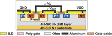
    Fig. 1. (Color online) The CMOS circuit configuration that is used in this work
    (Color online) The proposed metal interconnect strategy for fabricating the SiC NMOS and PMOS devices.
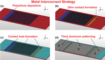
    Fig. 2. (Color online) The proposed metal interconnect strategy for fabricating the SiC NMOS and PMOS devices.
    (Color online) The doping profiles of N+, P-well and P+ regions obtained by process simulations through Synopsys Sentaurus.
    Fig. 3. (Color online) The doping profiles of N+, P-well and P+ regions obtained by process simulations through Synopsys Sentaurus.
    (Color online) The fabricated SiC NMOS, PMOS and CMOS gates. (a) PMOS. (b) NMOS. (c) Inverter gate. (d) NAND gate.
    Fig. 4. (Color online) The fabricated SiC NMOS, PMOS and CMOS gates. (a) PMOS. (b) NMOS. (c) Inverter gate. (d) NAND gate.
    (Color online) The measured transfer characteristics of the PMOS and NMOS.
    Fig. 5. (Color online) The measured transfer characteristics of the PMOS and NMOS.
    (Color online) (a) The typical measured voltage transfer curves and (b) the extracted inverter gain of the fabricated Inverter gate.
    Fig. 6. (Color online) (a) The typical measured voltage transfer curves and (b) the extracted inverter gain of the fabricated Inverter gate.
    (Color online) The measured switching input-output characteristics of the fabricated SiC Inverter gate.
    Fig. 7. (Color online) The measured switching input-output characteristics of the fabricated SiC Inverter gate.
    (Color online) The measured switching input-output characteristics of the fabricated SiC NAND gate.
    Fig. 8. (Color online) The measured switching input-output characteristics of the fabricated SiC NAND gate.
    ItemTemperature (°C)Energy (keV)
    P-well500550
    500360
    500200
    P+500320
    500200
    50040
    N+500160
    500130
    50040
    Table 1. The temperature, dose and energy used in the fabrications for P-well, P+ region and N+ regions.
    Tongtong Yang, Yan Wang, Ruifeng Yue. Demonstration of 4H-SiC CMOS digital IC gates based on the mainstream 6-inch wafer processing technique[J]. Journal of Semiconductors, 2022, 43(8): 082801
    Download Citation