Abstract
In this article, the design, fabrication and characterization of silicon carbide (SiC) complementary-metal-oxide-semiconductor (CMOS)-based integrated circuits (ICs) are presented. A metal interconnect strategy is proposed to fabricate the fundamental N-channel MOS (NMOS) and P-channel MOS (PMOS) devices that are required for the CMOS circuit configuration. Based on the mainstream 6-inch SiC wafer processing technology, the simultaneous fabrication of SiC CMOS ICs and power MOSFET is realized. Fundamental gates, such as inverter and NAND gates, are fabricated and tested. The measurement results show that the inverter and NAND gates function well. The calculated low-to-high delay (low-to-high output transition) and high-to-low delay (high-to-low output transition) are 49.9 and 90 ns, respectively.In this article, the design, fabrication and characterization of silicon carbide (SiC) complementary-metal-oxide-semiconductor (CMOS)-based integrated circuits (ICs) are presented. A metal interconnect strategy is proposed to fabricate the fundamental N-channel MOS (NMOS) and P-channel MOS (PMOS) devices that are required for the CMOS circuit configuration. Based on the mainstream 6-inch SiC wafer processing technology, the simultaneous fabrication of SiC CMOS ICs and power MOSFET is realized. Fundamental gates, such as inverter and NAND gates, are fabricated and tested. The measurement results show that the inverter and NAND gates function well. The calculated low-to-high delay (low-to-high output transition) and high-to-low delay (high-to-low output transition) are 49.9 and 90 ns, respectively.1. Introduction
Although silicon carbide (SiC) power devices have been proven to be stable and reliable for high temperature operation, the present control and drive circuits are based on silicon material, which restricts the maximum operating temperature of the power electronics system[1]. Developing SiC integrated circuits (ICs) is beneficial for realizing the full potential of SiC material in high temperature applications[2-6]. Compared with other technology, the complementary-metal-oxide-semiconductor (CMOS) technology could achieve full rail-to-rail output voltage switching, low power losses and temperature-independent logic levels[7, 8]. Unfortunately, the reported SiC CMOS ICs in the literature are fabricated using specially developed technology, which is not compatible with the mainstream 4H-SiC power device processing technology.
Motivated by developing 4H-SiC based power ICs which integrates the control circuits and power device in a single chip, this article reports the implementation of fundamental CMOS-based digital gates based on 6-inch SiC wafer processing technology, in which the digital gates and power devices are fabricated simultaneously. The fundamental characteristics of the inverter and NAND gates are characterized and analyzed. The experimental results that are obtained by this work will serve as useful guides for driving the development of SiC-based power ICs.
2. Device fabrication
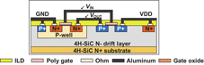
The CMOS circuit requires both N-channel MOS (NMOS) and P-channel MOS (PMOS) devices. To implement the SiC NMOS and PMOS while ensuring compatibility with the SiC power device processing technology, the CMOS configuration in Fig. 1 is adopted [7, 8]. The PMOS is formed directly in the drift layer, while the NMOS is fabricated in a P-well. The P-well also functions as a base layer for the SiC power MOSFET.

Figure 1.(Color online) The CMOS circuit configuration that is used in this work
Table Infomation Is Not Enable
In fabricating the SiC power MOSFET, only one thick metal is used for the cell interconnect [9]. In this work, a metal interconnect strategy is proposed to implement the CMOS circuits. The proposed metal interconnect strategy is shown in Fig. 2. The polysilicon acts as the gate (G) and the ohmic metal is extended to the other side to form the source (S), as shown in Figs. 2(a) and 2(b), respectively. After depositing the interlayer dielectric, contact holes are etched, as shown in Fig. 2(c). After sputtering the thick Aluminum metal, the wet etching technique is used to form the three electrodes, as shown in Fig. 2(d). The fabrications of SiC NMOS and PMOS are thus finished. The channel length for both NMOS and PMOS is 2 μm. The gate oxide thickness is 50 nm.
Figure 2.(Color online) The proposed metal interconnect strategy for fabricating the SiC NMOS and PMOS devices.
High temperature and high energy aluminum implantations and nitrogen implantations are used to form the P-wells, P+ regions and N+ regions, respectively. The process conditions for the implantations are summarized in Table 1. The obtained doping profiles for these regions are shown in Fig. 3. The depth of P-well should be larger than that of N+ region because the NMOS is located in the P-well.
Figure 3.(Color online) The doping profiles of N+, P-well and P+ regions obtained by process simulations through Synopsys Sentaurus.
3. Results and discussions
Based on the mainstream 6-inch SiC wafer processing technology, we realized the simultaneous fabrication of SiC digital gates and a SiC power MOSFET. Fig. 4 gives the photos of the fabricated SiC NMOS, PMOS and the CMOS gates. As shown in Figs. 4(a) and 4(b), the drain (D), gate (G) and source (S) of the NMOS and PMOS are clearly distinguished. The Inverter gate shown in Fig. 4(c) contains both PMOS and NMOS device, and the NAND gate in Fig. 4(d) integrates four devices. The measured transfer characteristics of the PMOS and NMOS are shown in Fig. 5. The typical threshold voltage Vth of the PMOS is 8.2 V while that of the NMOS is only 2.1 V. The asymmetry of Vth between PMOS and NMOS should be attributed to the unavoidable fixed charges located at the interface of SiC and SiO2[10].
Figure 4.(Color online) The fabricated SiC NMOS, PMOS and CMOS gates. (a) PMOS. (b) NMOS. (c) Inverter gate. (d) NAND gate.
Figure 5.(Color online) The measured transfer characteristics of the PMOS and NMOS.
After bonding the fabricated inverter and NAND gates, the functions of the two gates are evaluated. The measured voltage transfer curves of the inverter gate at various VDDs are shown in Fig. 6(a). The inverter gate functions are as expected. We also extract the inverter gain from the voltage transfer curves and the results are shown in Fig. 6(b). It is found that the inverter gain increases with VDD. At a VDDof 15 V, the inverter gain is larger than 50, which is beneficial for fabricating more complex integrated circuits, such as a multi-stage ring oscillator.
Figure 6.(Color online) (a) The typical measured voltage transfer curves and (b) the extracted inverter gain of the fabricated Inverter gate.
Fig. 7 give the typical measured input-output voltage curves of the inverter gate. The obtained waveform demonstrates that the inverter gate functions well. In addition, from the voltage curves, the calculated low-to-high delay tpLH (low-to-high output transition) and high-to-low delay tpHL (high-to-low output transition) are 49.9 and 90 ns, respectively. The measured dynamic switching characteristic of the NAND gate is shown in Fig. 8. Obviously, the obtained results verify the normal operation of the NAND gate.
Image Infomation Is Not Enable
Figure 1.(Color online) The CMOS circuit configuration that is used in this work
The fabricated SiC power MOSFET is of a trench structure. The related experimental results have been reported in Ref. [11]. Based on the proposed metal interconnect strategy, the SiC IC gates and trench power MOSFET are fabricated on the same wafer. It is expected that SiC power ICs which integrate the SiC ICs and a power MOSFET will be realized in future work.
4. Conclusion
In this article, 4H-SiC CMOS digital gates are successfully fabricated based on the mainstream SiC processing technology. The functions of the inverter and NAND gate are verified through experimental measurements. Based on these fundamental gates, more complex SiC CMOS based integrated circuits can be fabricated. Moreover, the simultaneous fabrication of the SiC CMOS circuits and power MOSFET can be realized. Therefore, the results of this research can provide valuable guides for the future fabrication of power integrated circuits to realize the full potential of SiC power devices in high temperature applications.
Acknowledgements
The authors would like to thank State Key Laboratory of Advanced Power Transmission Technology, Global Energy Interconnection Research Institute Co. Ltd. for the fabrication of the SiC trench MOSFET and Datang Microelectronics Technology limited Company for wafer dicing.
References
[1] R C Murphree, S Roy, S Ahmed et al. A SiC CMOS linear voltage regulator for high-temperature applications. IEEE Trans Power Electron, 35, 913(2020).
[2] L Lanni, B G Malm, M Östling et al. 500 °C bipolar integrated OR/NOR gate in 4H-SiC. IEEE Electron Device Lett, 34, 1091(2013).
[3] A S Kashyap, C P Chen, R Ghandi et al. Silicon carbide integrated circuits for extreme environments. The 1st IEEE Workshop on Wide Bandgap Power Devices and Applications, 60(2013).
[4] J Y Lee, S Singh, J A Cooper. Demonstration and characterization of bipolar monolithic integrated circuits in 4H-SiC. IEEE Trans Electron Devices, 55, 1946(2008).
[5] K Sheng, Y X Zhang, M Su et al. Demonstration of the first SiC power integrated circuit. Solid State Electron, 52, 1636(2008).
[6] M Alexandru, V Banu, X Jorda et al. SiC integrated circuit control electronics for high-temperature operation. IEEE Trans Ind Electron, 62, 3182(2015).
[7] S H Ryu, K T Kornegay, J A Cooper et al. Digital CMOS IC's in 6H-SiC operating on a 5-V power supply. IEEE Trans Electron Devices, 45, 45(1998).
[8] M Okamoto, A Yao, H Sato et al. First demonstration of a monolithic SiC power IC integrating a vertical MOSFET with a CMOS gate buffer. 2021 33rd International Symposium on Power Semiconductor Devices and ICs, 71(2021).
[9] R H Huang, Y H Tao, S Bai et al. Design and fabrication of a 3.3 kV 4H-SiC MOSFET. J Semicond, 36, 094002(2015).
[10] G D Licciardo, L di Benedetto, S Bellone. Modeling of the SiO2/SiC interface-trapped charge as a function of the surface potential in 4H-SiC vertical-DMOSFET. IEEE Trans Electron Devices, 63, 1783(2016).
[11] T T Yang, X B Li, Y Wang et al. Design and fabrication of 860V SiC trench MOSFET with stripe and rectangular cells. 2021 IEEE International Conference on Integrated Circuits, Technologies and Applications, 161(2021).