
Sai Jiang, Qinyong Dai, Jianhang Guo, Yun Li. In-situ/operando characterization techniques for organic semiconductors and devices[J]. Journal of Semiconductors, 2022, 43(4): 041101
- Journal of Semiconductors
- Vol. 43, Issue 4, 041101 (2022)
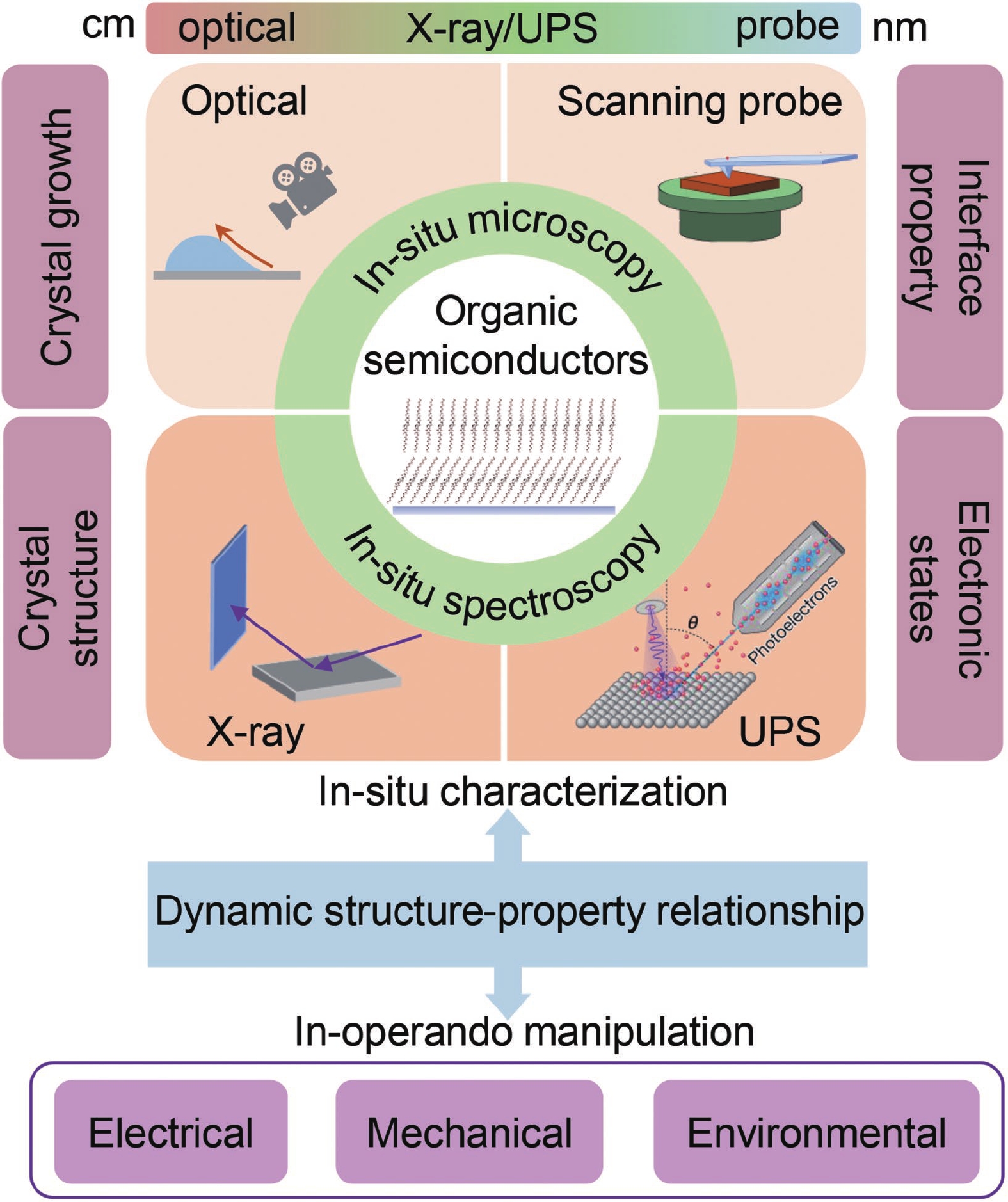
Fig. 1. (Color online) Overview of various in-situ characterization techniques with different resolutions, from centimeter to nanometer, to study the dynamic structure-property relationship under manipulation.
![(Color online) In-situ optical microscopy for characterizations of organic crystalline films. (a) Schematic diagram of CoMiC-based analytical system along the entire flow path connecting flow pattern, crystallization, and thin-film properties (upper panel of (a)). Side-view in-situ image analysis of meniscus shape variation during the coating (lower panel of (a)). (b) In-situ microscopy images showing the variation of solution/thin-film boundary and crystallization process of doped TIPS-pentacene using the FM-CoMiC and the SHM-CoMiC[22]. (c) Schematic diagram of top-view and side-view in-situ microscopy to investigate the relationship between 3D meniscus geometry and crystallization during solution shearing. (d) The top-, side-, and 3D-view microscopies for the visualization of the contact line/crystallization process and cross-sectional meniscus shape[34].](/richHtml/jos/2022/43/4/041101/img_2.jpg)
Fig. 2. (Color online) In-situ optical microscopy for characterizations of organic crystalline films. (a) Schematic diagram of CoMiC-based analytical system along the entire flow path connecting flow pattern, crystallization, and thin-film properties (upper panel of (a)). Side-view in-situ image analysis of meniscus shape variation during the coating (lower panel of (a)). (b) In-situ microscopy images showing the variation of solution/thin-film boundary and crystallization process of doped TIPS-pentacene using the FM-CoMiC and the SHM-CoMiC[22 ]. (c) Schematic diagram of top-view and side-view in-situ microscopy to investigate the relationship between 3D meniscus geometry and crystallization during solution shearing. (d) The top-, side-, and 3D-view microscopies for the visualization of the contact line/crystallization process and cross-sectional meniscus shape[34 ].
Fig. 3. (Color online) In-situ AFM characterizations. (a) Evolutionary selection growth approach and time-lapse sequence of representative AFM images showing the morphological evolution of the precursors on the SiO2 surface. Scale bar: 2 μ m[38 ]. (b) Schematic illustration of the experimental setup for in-situ AFM imaging with perfusion flow of the guest solution. (c) 1.0 × 1.0 µ m2 topographic images of the PCP surface taken at the indicated times under the perfusion flow of a 200 mM bpy solution with a constant flow rate. The high-resolution parts are 30 × 30 nm2 phase images of the liquid–solid interface taken at lattice scale[21 ].
Fig. 4. (Color online) (a) Device cross-section schematic showing the working principle of (left) OFETs, (middle) EGOFETs, and (right) OECTs[52 ]. (b) AFM images (10 × 10 µ m2) of n-type films (upper) P-90 and (lower) BBL. The films were immersed in 0.1 M NaCl at different conditions[16 ]. (c) Instrumentation schematic of in-situ ESM using dual-amplitude resonance tracking centered around the contact resonance frequency. Schematics of different electrochemical transistor operating modes in the AFM experiment (lower). (d) Topography and ESM amplitude images of a typical P3HT film in 20 mM KCl. (e) AM–FM stiffness map (frequency) with a line-flattened processing[20 ]. (f) In-liquid SDM setup for the nanoscale electrical characterization of a functional EGOFET. (g) Constant height electric force images expressed in capacitance gradient (64 × 13 pixels) at 180 nm. (h) Conductivity maps of the central part of the channel. (i) Topographic and mechanical phase of a different region of the channel measured in intermittent contact mode. Constant height electrical image of the same region for the transistor in-operando[37 ].
Fig. 5. (Color online) In-situ X-ray characterization techniques. (a) Conceptual representation of the in-situ solution-shearing system. (b) Scattering regions captured by the high-speed GIWAXS detector for a representative solution-sheared TIPS-pentacene thin film[71 ]. (c) Schematic view of in-situ stretching GIXD experimental setup and in-situ measurements of the structure and strain of a π-conjugated semiconducting polymer under mechanical load[72 ]. Schematic representation of (d) nano-GIXD setup, (e) bottom contact OFET stack, and (f) typical diffraction patterns at polymer channel and electrode position[73 ].
Fig. 6. (Color online) In-situ ultraviolet photoelectron spectroscopy. (a) Experimental design to examine the behavior of PE and MWNT/PEDOT:PSS films before and after high-temperature annealing[80 ]. (b) Schematic diagram of the photoelectron spectroscopy setup with UV He II as the photon source. Upon irradiation with energy hv , photoelectrons are injected from the organic semiconductor sample via the photoelectric effect. (c) Energy level diagram of an organic semiconductor showing electrons being photoejected from a HOMO level to a state above the vacuum level with a finite kinetic energy. (d) Schematic diagram showing the experimental design used for in-situ ultraviolet photoelectron spectroscopy measurements[81 ].

Set citation alerts for the article
Please enter your email address
© Copyright 2018-2021 | Chinese Laser Press. All Rights Reserved 沪ICP备15018463号-20