• Journal of Semiconductors
  • Vol. 43, Issue 5, 051202 (2022)
Wanlong Wang1, Dongyang Zhang2, Rong Liu1, Deepak Thrithamarassery Gangadharan2, Furui Tan1, and Makhsud I. Saidaminov2
Author Affiliations
  • 1Key Laboratory of Photovoltaic Materials, Henan University, Kaifeng 475004, China
  • 2Department of Chemistry, Department of Electrical & Computer Engineering, and Centre for Advanced Materials and Related Technologies (CAMTEC), University of Victoria, Victoria, British Columbia V8P 5C2, Canada
  • show less
    DOI: 10.1088/1674-4926/43/5/051202 Cite this Article
    Wanlong Wang, Dongyang Zhang, Rong Liu, Deepak Thrithamarassery Gangadharan, Furui Tan, Makhsud I. Saidaminov. Characterization of interfaces: Lessons from the past for the future of perovskite solar cells[J]. Journal of Semiconductors, 2022, 43(5): 051202 Copy Citation Text show less
    (Color online) Efficiency evolution of different solar cells. Interface engineering has recently played an increasingly important role in obtaining a higher efficiency for each cell.
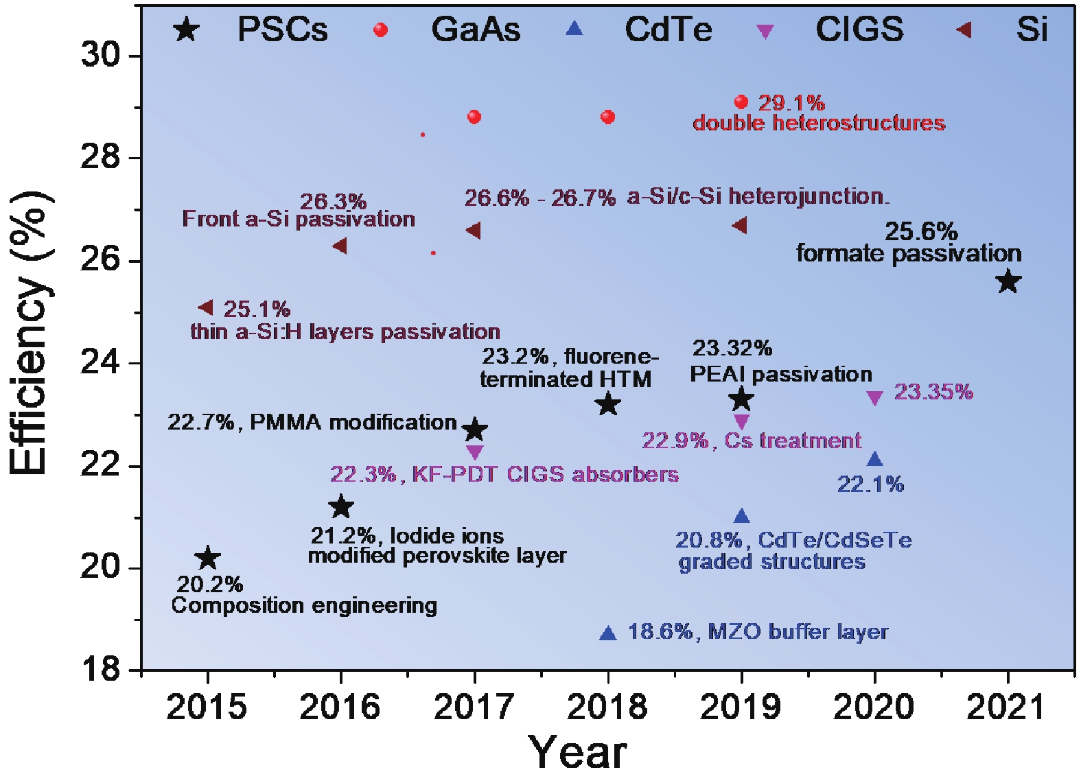
    Fig. 1. (Color online) Efficiency evolution of different solar cells. Interface engineering has recently played an increasingly important role in obtaining a higher efficiency for each cell.
    (Color online) (a) Perovskite crystal structure, Schottky defect, Frenkel defect and ion migration through interfaces. (b) Schematic illustration of photo-generation and, diffusion and transfer of charges at interfaces, trap-assisted nonradiative recombination (due to intrinsic defects and impurities at interfaces) and back transfer and interface recombination. (c) Energy band alignment of some typical materials used in perovskite solar cells.
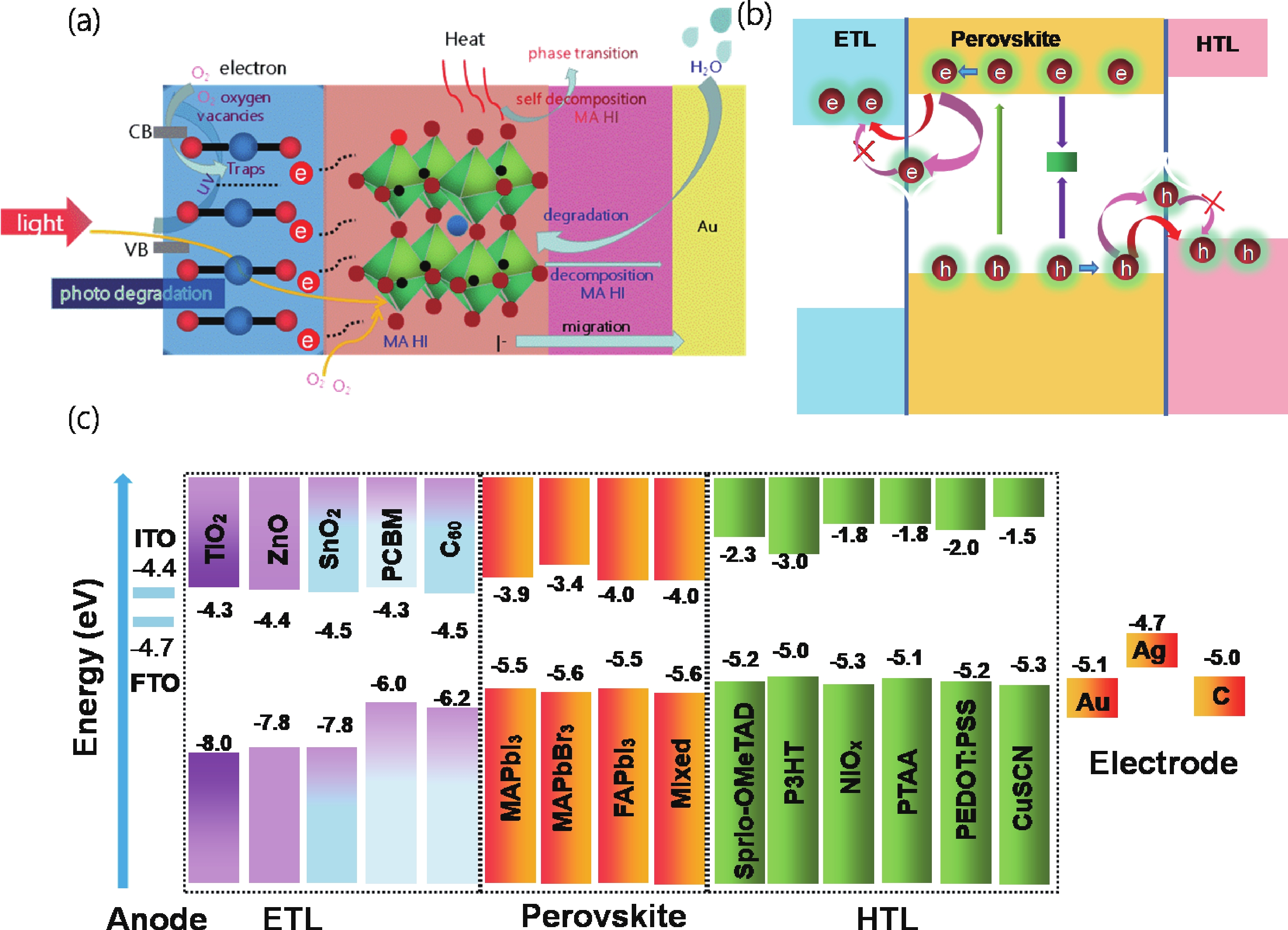
    Fig. 2. (Color online) (a) Perovskite crystal structure, Schottky defect, Frenkel defect and ion migration through interfaces. (b) Schematic illustration of photo-generation and, diffusion and transfer of charges at interfaces, trap-assisted nonradiative recombination (due to intrinsic defects and impurities at interfaces) and back transfer and interface recombination. (c) Energy band alignment of some typical materials used in perovskite solar cells.
    (Color online) Interface material characterization methods. (a) Cross-section SEM image of PSCs showing excess of PbI2 at interfaces. Reproduced with permission from Ref. [84]. Copyright 2019, ACS. (b) Photoluminescence mapping image showing the crystallization of perovskite from the pre-embedded perovskite seeds. Reproduced with permission from Ref. [89]. Copyright 2018, Nature. (c) AFM image of TiO2. Reproduced with permission from Ref. [90]. Copyright 2020, RSC. (d) Cross-sectional HRTEM imagewide band gap perovskite near the surface. Scale bars: 1 μm. Reproduced with permission from Ref. [91]. Copyright 2019, Nature. (e) XPS depth profiles for cross-sectional characterization. Reproduced with permission from Ref. [95]. Copyright 2015, ACS. (f) and (g) Schematic illustration and measurement results from TOF-SIMS characterization. Reproduced with permission from Ref. [103]. Copyright 2018, Nature.
    Fig. 3. (Color online) Interface material characterization methods. (a) Cross-section SEM image of PSCs showing excess of PbI2 at interfaces. Reproduced with permission from Ref. [84]. Copyright 2019, ACS. (b) Photoluminescence mapping image showing the crystallization of perovskite from the pre-embedded perovskite seeds. Reproduced with permission from Ref. [89]. Copyright 2018, Nature. (c) AFM image of TiO2. Reproduced with permission from Ref. [90]. Copyright 2020, RSC. (d) Cross-sectional HRTEM imagewide band gap perovskite near the surface. Scale bars: 1 μm. Reproduced with permission from Ref. [91]. Copyright 2019, Nature. (e) XPS depth profiles for cross-sectional characterization. Reproduced with permission from Ref. [95]. Copyright 2015, ACS. (f) and (g) Schematic illustration and measurement results from TOF-SIMS characterization. Reproduced with permission from Ref. [103]. Copyright 2018, Nature.
    (Color online) (a) Steady state and (b) time resolved photoluminescence (PL) spectra of perovskite films with different back contact layers. Reproduced with permission from Ref. [105]. Copyright 2018, Wiley. (c) Transmission (ΔT/T) spectra of devices. Reproduced with permission from Ref. [122]. Copyright 2020, ELSEVIER. (d) Transient absorption kinetics of perovskite films with different substrates. Reproduced with permission from Ref. [124]. Copyright 2015, ACS. (e) Ultraviolet photoelectron spectroscopy (UPS) spectra showing the energy-level alignment of the interfaces. Reproduced with permission from Ref. [125]. Copyright 2020, Wiley. (f) Reflectivity spectra of perovskite films on textured substrates. Reproduced with permission from Ref. [128]. Copyright 2019, ACS.
    Fig. 4. (Color online) (a) Steady state and (b) time resolved photoluminescence (PL) spectra of perovskite films with different back contact layers. Reproduced with permission from Ref. [105]. Copyright 2018, Wiley. (c) Transmission (ΔT/T) spectra of devices. Reproduced with permission from Ref. [122]. Copyright 2020, ELSEVIER. (d) Transient absorption kinetics of perovskite films with different substrates. Reproduced with permission from Ref. [124]. Copyright 2015, ACS. (e) Ultraviolet photoelectron spectroscopy (UPS) spectra showing the energy-level alignment of the interfaces. Reproduced with permission from Ref. [125]. Copyright 2020, Wiley. (f) Reflectivity spectra of perovskite films on textured substrates. Reproduced with permission from Ref. [128]. Copyright 2019, ACS.
    (Color online) (a) Transient photocurrent spectra of perovskite films with different contact thin layers. Reproduced with permission from Ref. [105]. Copyright 2019, Wiley. The energy-level alignments at interface are also given for comparison. Reproduced with permission from Ref. [134]. Copyright 2019, Wiley. (b) Transient photovoltage spectra of perovskite films with different TiO2 ETL. The inset shows the contact passivation of perovskite by interfacial Cl. Reproduced with permission from Ref. [60]. Copyright 2017, Science. (c) Charge transfer recombination resistance at different bias voltages in electrochemical impedance spectrum measurement. Reproduced with permission from Ref. [146]. Copyright 2020, Wiley. (d) Space-charge-limited current (SCLC) characterization of perovskite solar cells with different SnO2 ETLs. Reproduced with permission from Ref. [153]. Copyright 2020, Wiley. (e) Electron beam induced current (EBIC) measurement of the current mapping at cross-section interfaces. Reproduced with permission from Ref. [160]. Copyright 2019, Science.
    Fig. 5. (Color online) (a) Transient photocurrent spectra of perovskite films with different contact thin layers. Reproduced with permission from Ref. [105]. Copyright 2019, Wiley. The energy-level alignments at interface are also given for comparison. Reproduced with permission from Ref. [134]. Copyright 2019, Wiley. (b) Transient photovoltage spectra of perovskite films with different TiO2 ETL. The inset shows the contact passivation of perovskite by interfacial Cl. Reproduced with permission from Ref. [60]. Copyright 2017, Science. (c) Charge transfer recombination resistance at different bias voltages in electrochemical impedance spectrum measurement. Reproduced with permission from Ref. [146]. Copyright 2020, Wiley. (d) Space-charge-limited current (SCLC) characterization of perovskite solar cells with different SnO2 ETLs. Reproduced with permission from Ref. [153]. Copyright 2020, Wiley. (e) Electron beam induced current (EBIC) measurement of the current mapping at cross-section interfaces. Reproduced with permission from Ref. [160]. Copyright 2019, Science.
    Wanlong Wang, Dongyang Zhang, Rong Liu, Deepak Thrithamarassery Gangadharan, Furui Tan, Makhsud I. Saidaminov. Characterization of interfaces: Lessons from the past for the future of perovskite solar cells[J]. Journal of Semiconductors, 2022, 43(5): 051202
    Download Citation