• Journal of Semiconductors
  • Vol. 43, Issue 6, 062804 (2022)
Xuemin Zhang1、2, Changling Yan1, Jinghang Yang1, Chao Pang1, Yunzhen Yue1, Chunhong Zeng1、2, and Baoshun Zhang2
Author Affiliations
  • 1State Key Laboratory on High Power Semiconductor Lasers, Changchun University of Science and Technology, Changchun 130022, China
  • 2Nanofabrication Facility, Suzhou Institute of Nano-Tech and Nano-Bionics, Chinese Academy of Sciences, Suzhou 215123, China
  • show less
    DOI: 10.1088/1674-4926/43/6/062804 Cite this Article
    Xuemin Zhang, Changling Yan, Jinghang Yang, Chao Pang, Yunzhen Yue, Chunhong Zeng, Baoshun Zhang. Vertical Schottky ultraviolet photodetector based on graphene and top–down fabricated GaN nanorod arrays[J]. Journal of Semiconductors, 2022, 43(6): 062804 Copy Citation Text show less
    (Color online) (a) The process schematic diagram of the preparation of GaN nanorods. (b) The PL spectra of GaN before and after graphene transfer. (c) The Raman spectra of graphene grown on copper foil.
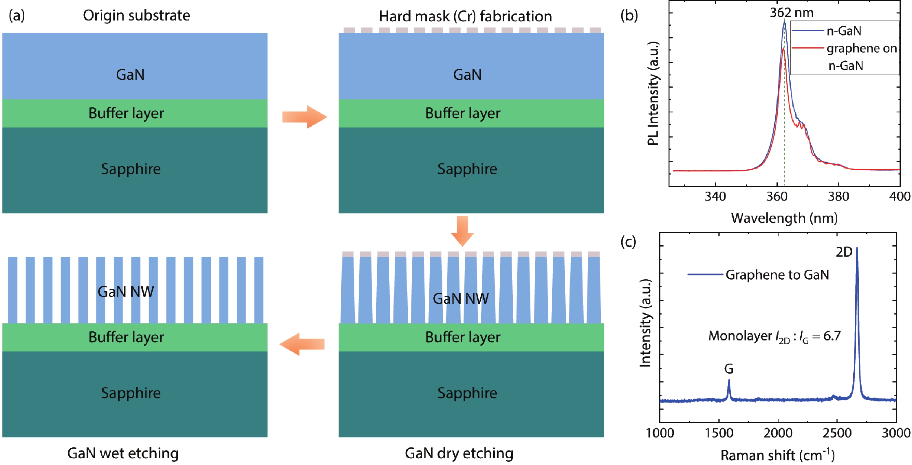
    Fig. 1. (Color online) (a) The process schematic diagram of the preparation of GaN nanorods. (b) The PL spectra of GaN before and after graphene transfer. (c) The Raman spectra of graphene grown on copper foil.
    The basic process of GaN nanorod formation by SEM at different etching time: (a) 3, (b) 5, (c) 10, (d) 15, (e) 17, and (f) 22 min.
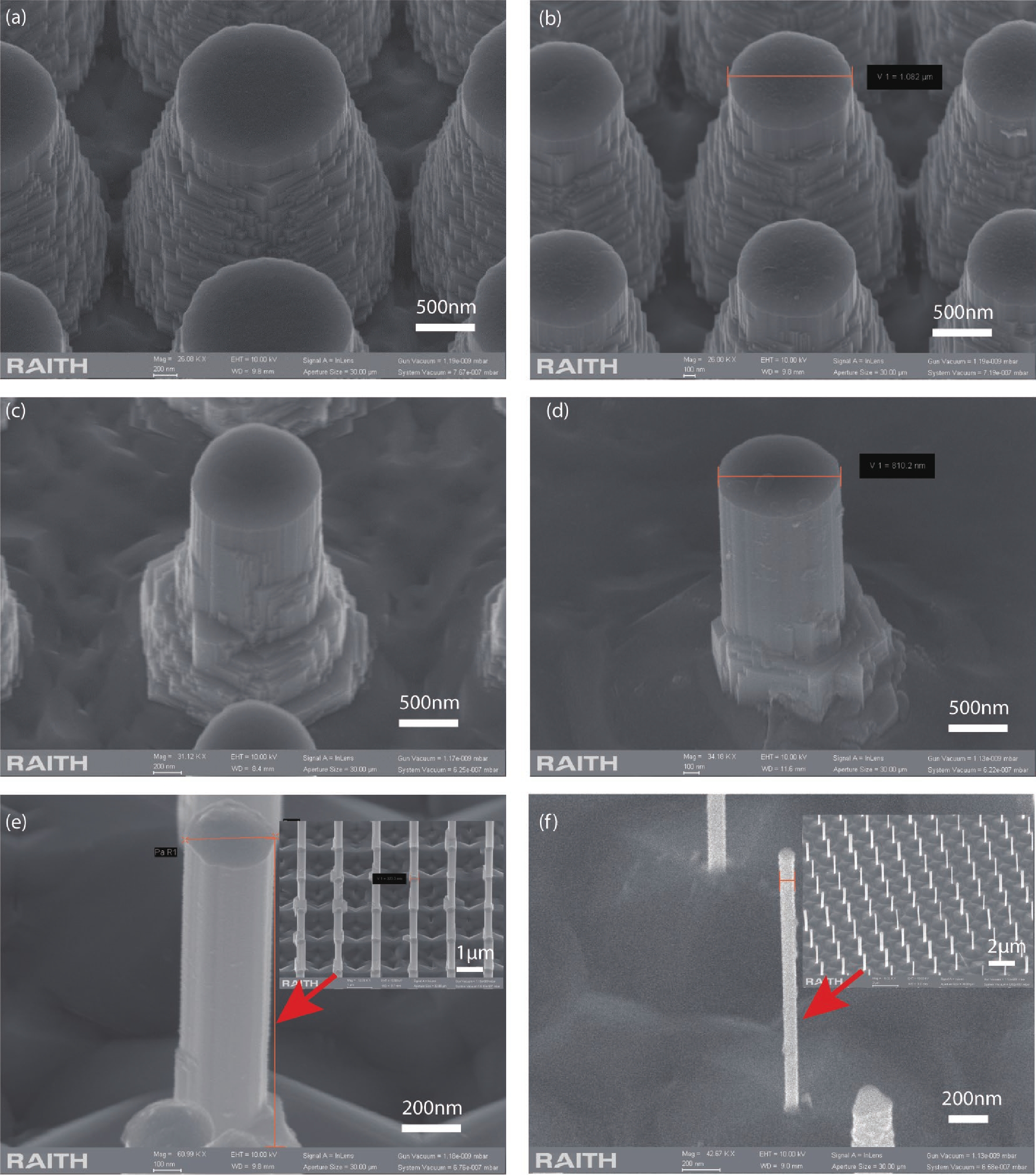
    Fig. 2. The basic process of GaN nanorod formation by SEM at different etching time: (a) 3, (b) 5, (c) 10, (d) 15, (e) 17, and (f) 22 min.
    (Color online) (a) The cross-sectional structure of the graphene–GaN nanorod array heterojunction ultraviolet detector. (b) An optical microscope image of the device structure, and the inset is an SEM image of GaN nanorods. (c, d) The I–V characteristics of graphene–GaN nanorods photodetectors in darkness and light. (e, f) The variation of current with time at the bias of –5 V under the cyclic ultraviolet illumination of the detector.
    Fig. 3. (Color online) (a) The cross-sectional structure of the graphene–GaN nanorod array heterojunction ultraviolet detector. (b) An optical microscope image of the device structure, and the inset is an SEM image of GaN nanorods. (c, d) The IV characteristics of graphene–GaN nanorods photodetectors in darkness and light. (e, f) The variation of current with time at the bias of –5 V under the cyclic ultraviolet illumination of the detector.
    (Color online) (a) The band structure of the graphene–GaN nanorod array heterostructure. (b) A curve of device photoresponsivity as bias voltage changes. (c) The bias voltage and light power as a function of D*. (d) The spectral response curve of the detector at the bias of –5 V.
    Fig. 4. (Color online) (a) The band structure of the graphene–GaN nanorod array heterostructure. (b) A curve of device photoresponsivity as bias voltage changes. (c) The bias voltage and light power as a function of D*. (d) The spectral response curve of the detector at the bias of –5 V.
    MaterialResponse band (nm)Bias (V)Responsivity (A/W)EQE (%)D* (Jones) τr/τf (ms) Ref.
    G-GaN NW357125[14]
    G-GaAs NW53200.001540.071/0.194[30]
    G-Ga2O3 NW 258/365–53 × 104/0.185 9/8[31]
    G-GaN325100.3687.51 × 10105.05/5.11[17]
    G-AlGaN/GaN300/350–20.56/0.079[32]
    G-GaN NR360–513.94791.44 × 101013/8This work
    Table 1. The performance comparison of graphene (G) and Ga-based materials heterostructure photodetectors.
    Xuemin Zhang, Changling Yan, Jinghang Yang, Chao Pang, Yunzhen Yue, Chunhong Zeng, Baoshun Zhang. Vertical Schottky ultraviolet photodetector based on graphene and top–down fabricated GaN nanorod arrays[J]. Journal of Semiconductors, 2022, 43(6): 062804
    Download Citation